
Page 63 - MEMS and Microstructures in Aerospace Applications
P. 63
Osiander / MEMS and microstructures in Aerospace applications DK3181_c003 Final Proof page 53 1.9.2005 8:59pm
MEMS Fabrication 53
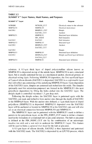
TABLE 3.5
SUMMiT Ve Layer Names, Mask Names, and Purposes
SUMMiT Ve Layer Mask Purpose
NITRIDE NITRIDE_CUT Electrical contact to the substrate
MMPOLY0 MMPOLY0 Electrical interconnect
SACOX1 DIMPLE1_CUT Dimple
SACOX1_CUT Anchors
MMPOLY1 MMPOLY1 Structural layer definition
PIN_JOINT Hub formation
SACOX2 SACOX2 Hub formation
MMPOLY2 MMPOLY2 Structural layer
SACOX3 DIMPLE3_CUT Anchors
SACOX3_CUT
SACOX3 Dimple
MMPOLY3 MMPOLY3 Structural layer definition
SACOX4 DIMPLE4_CUT Dimple sacrificial layer definition
SACOX4_CUT
MMPOLY4 MMPOLY4 Structural layer definition
substrate. A 0.3-mm thick layer of doped polycrystalline silicon known as
MMPOLY0 is deposited on top of the nitride layer. MMPOLY0 is not a structural
layer, but is usually patterned for use as a mechanical anchor, electrical ground, or
electrical wiring layer. Following MMPOLY0 deposition, the first sacrificial layer
of 2 mm of silicon dioxide (SACOX1) is deposited. SACOX1 is a conformable layer
that will reflect any patterning of the underlying MMPOLY0 layer. Upon deposition
of the SACOX1 layer, dimples are patterned and etched into the oxide. The dimples
(primarily used for antistiction purposes) are formed in the MMPOLY1 (the next
polysilicon deposition) by filling the holes etched into the SACOX1 layer. The
dimple depth is controlled via timed 1.5 mm deep etch.
Following the dimple etches, the SACOX1 layer is patterned again with the
SACOX1_cut mask and etched to form anchor sites through the depth of SACOX1
to the MMPoly0 layer. With the anchor sites defined, a 1-mm thick layer of doped
polysilicon (MMPOLY1) is deposited. MMPOLY1 deposited over the SACOX1
layer will be anchored or bonded to MMPOLY0 at the SACOX1 cuts and will also
act as an electrical connection between MMPOLY0 and MMPOLY1.
The MMPOLY1 layer can be patterned with the MMPOLY1 mask to define a
pattern in the polysilicon layer, or the PIN_JOINT_CUT mask to define a feature
used in the formation of a rotational hub or pin-joint structure. The hub or pin-joint
is defined at the PIN_JOINT_CUT site by the combination of an anisotropic
reactive ion etch and a wet etch to undercut the MMPOLY1 layer. This feature
will be used to form a captured rivet head for the hub or pin-joint.
A 0.3-mm layer of silicon dioxide, SACOX2 is then deposited and patterned
with the SACOX2 mask. The SACOX2 is deposited by an LPCVD process, which
© 2006 by Taylor & Francis Group, LLC