
Page 61 - MEMS and Microstructures in Aerospace Applications
P. 61
Osiander / MEMS and microstructures in Aerospace applications DK3181_c003 Final Proof page 51 1.9.2005 8:59pm
MEMS Fabrication 51
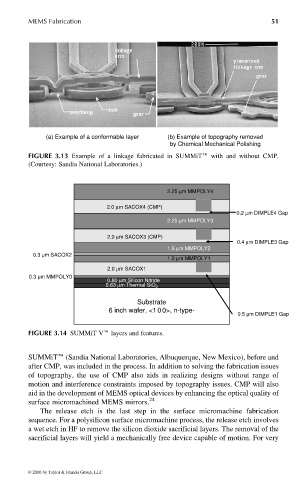
(a) Example of a conformable layer (b) Example of topography removed
by Chemical Mechanical Polishing
FIGURE 3.13 Example of a linkage fabricated in SUMMiTe with and without CMP.
(Courtesy: Sandia National Laboratories.)
2.25 µm MMPOLY4
2.0 µm SACOX4 (CMP)
0.2 µm DIMPLE4 Gap
2.25 µm MMPOLY3
2.0 µm SACOX3 (CMP)
0.4 µm DIMPLE3 Gap
1.5 µm MMPOLY2
0.3 µm SACOX2
1.0 µm MMPOLY1
2.0 µm SACOX1
0.3 µm MMPOLY0
0.80 µm Silicon Nitride
0.63 µm Thermal SiO
2
Substrate
6 inch wafer, <10 0>, n-type-
0.5 µm DIMPLE1 Gap
FIGURE 3.14 SUMMiT Ve layers and features.
SUMMiTe (Sandia National Laboratories, Albuquerque, New Mexico), before and
after CMP, was included in the process. In addition to solving the fabrication issues
of topography, the use of CMP also aids in realizing designs without range of
motion and interference constraints imposed by topography issues. CMP will also
aid in the development of MEMS optical devices by enhancing the optical quality of
24
surface micromachined MEMS mirrors.
The release etch is the last step in the surface micromachine fabrication
sequence. For a polysilicon surface micromachine process, the release etch involves
a wet etch in HF to remove the silicon dioxide sacrificial layers. The removal of the
sacrificial layers will yield a mechanically free device capable of motion. For very
© 2006 by Taylor & Francis Group, LLC