
Page 57 - MEMS and Microstructures in Aerospace Applications
P. 57
Osiander / MEMS and microstructures in Aerospace applications DK3181_c003 Final Proof page 47 1.9.2005 8:59pm
MEMS Fabrication 47
Howe and Muller 18 provided a basic definition of polycrystalline silicon surface
micromachining, and Fan et al. 19 illustrated an array of mechanical elements such
as fixed-axle pin joints, self-constraining pin joints, and sliding elements. Pister
et al. 20 demonstrated the design for microfabricated hinges, which enable the
erection of optical mirror elements.
Surface micromachining is a fabrication technology based upon the deposition,
patterning, and etching of a stack of materials upon a substrate. The materials
consist of alternating layers of a structural material and a sacrificial material. The
sacrificial material is removed at the end of the fabrication process via a release
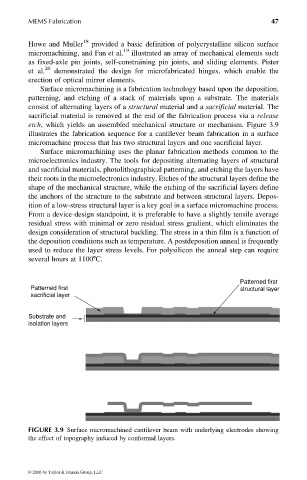
etch, which yields an assembled mechanical structure or mechanism. Figure 3.9
illustrates the fabrication sequence for a cantilever beam fabrication in a surface
micromachine process that has two structural layers and one sacrificial layer.
Surface micromachining uses the planar fabrication methods common to the
microelectronics industry. The tools for depositing alternating layers of structural
and sacrificial materials, photolithographical patterning, and etching the layers have
their roots in the microelectronics industry. Etches of the structural layers define the
shape of the mechanical structure, while the etching of the sacrificial layers define
the anchors of the structure to the substrate and between structural layers. Depos-
ition of a low-stress structural layer is a key goal in a surface micromachine process.
From a device-design standpoint, it is preferable to have a slightly tensile average
residual stress with minimal or zero residual stress gradient, which eliminates the
design consideration of structural buckling. The stress in a thin film is a function of
the deposition conditions such as temperature. A postdeposition anneal is frequently
used to reduce the layer stress levels. For polysilicon the anneal step can require
several hours at 11008C.
Patterned first
Patterned first structural layer
sacrificial layer
Substrate and
isolation layers
FIGURE 3.9 Surface micromachined cantilever beam with underlying electrodes showing
the effect of topography induced by conformal layers.
© 2006 by Taylor & Francis Group, LLC