
Page 55 - MEMS and Microstructures in Aerospace Applications
P. 55
Osiander / MEMS and microstructures in Aerospace applications DK3181_c003 Final Proof page 45 1.9.2005 8:59pm
MEMS Fabrication 45
The details and types of etch chemistries involved in plasma etching are varied and
quite complex. This topic is too voluminous to be discussed in detail here, but there
exist a number of excellent references on this subject. 15 The proper choice of these
chemistries produces various etch rates and selectivity of material etch rates, which is
essential to the integration of processes to produce microelectronics or MEMS devices.
Fluoride etch chemistries is one of the most widely studied for silicon etches. Equations
(3.3), (3.4), and (3.5) illustrate some of the fluoride reactions involved in the etching of
silicon, silicon dioxide, and silicon nitride, respectively. There are a number of feed
gases that can produce the free radicals involved in these reactions:
Si þ 4F ! SiF 4 (3:3)
þ
3SiO 2 þ 4CF ! 2CO þ 2CO 2 þ 3SiF 4 (3:4)
3
Si 3 N 4 þ 12F ! 3SiF 4 þ 2N 2 (3:5)
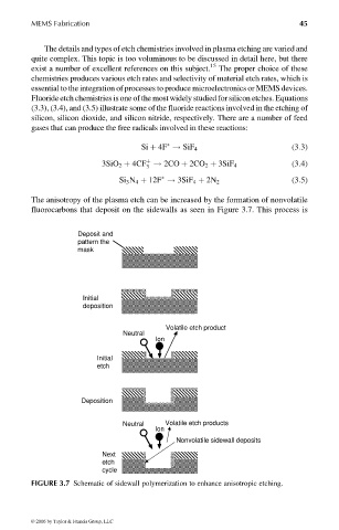
The anisotropy of the plasma etch can be increased by the formation of nonvolatile
fluorocarbons that deposit on the sidewalls as seen in Figure 3.7. This process is
Deposit and
pattern the
mask
Initial
deposition
Volatile etch product
Neutral
Ion
Initial
etch
Deposition
Neutral Volatile etch products
Ion
Nonvolatile sidewall deposits
Next
etch
cycle
FIGURE 3.7 Schematic of sidewall polymerization to enhance anisotropic etching.
© 2006 by Taylor & Francis Group, LLC