
Page 59 - MEMS and Microstructures in Aerospace Applications
P. 59
Osiander / MEMS and microstructures in Aerospace applications DK3181_c003 Final Proof page 49 1.9.2005 8:59pm
MEMS Fabrication 49
TABLE 3.4
A Comparison of MEMS and Microelectronics
Criteria Microelectronics MEMS
Feature size Sub-micron 1–3 mm
Device size Sub-micron ~50 mm to 1mm
Materials Silicon-based Varied (silicon, metals, plastics)
Fundamental devices Limited Set: Widely Varied:
Transistor, capacitor, resistor Fluidic, mechanical, optical, electrical elements
(sensors, actuators, switches, mirrors, etc.)
Fabrication process Standardized: Varied:
Planar silicon process Three main categories of MEMS
fabrication processes plus variants.
. Bulk micromachining
. Surface micromachining
. LIGA
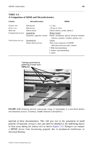
Topology generated by
patterning of lower level
(MMpoly0)
MMpoly2
MMpoly0
FIGURE 3.10 Scanning electron microscope image of topography in a two-level surface
micromachine process. (Courtesy: Sandia National Laboratories.)
material at these discontinuities. This will give rise to the generation of small
particles of material, stringers, that can either be attached to the underlying layers
or float away during the release etch as shown Figure 3.12. Stringers can hamper
a MEMS device from functioning properly due to mechanical interference or
electrical shorting.
© 2006 by Taylor & Francis Group, LLC