
Page 54 - MEMS and Microstructures in Aerospace Applications
P. 54
Osiander / MEMS and microstructures in Aerospace applications DK3181_c003 Final Proof page 44 1.9.2005 8:59pm
44 MEMS and Microstructures in Aerospace Applications
Container
Diffused or
implanted n-type
+ silicon region
P-type silicon
V
Mask
Etchant
Electrode Container
(a) Electrochemical Etch Schematic
(b) Completed Structure
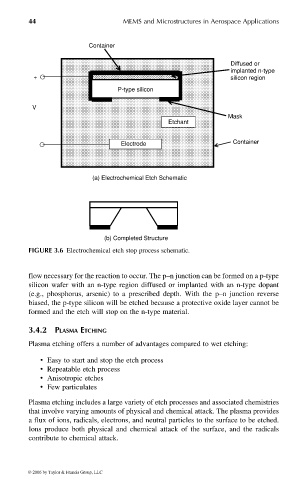
FIGURE 3.6 Electrochemical etch stop process schematic.
flow necessary for the reaction to occur. The p–n junction can be formed on a p-type
silicon wafer with an n-type region diffused or implanted with an n-type dopant
(e.g., phosphorus, arsenic) to a prescribed depth. With the p–n junction reverse
biased, the p-type silicon will be etched because a protective oxide layer cannot be
formed and the etch will stop on the n-type material.
3.4.2 PLASMA ETCHING
Plasma etching offers a number of advantages compared to wet etching:
. Easy to start and stop the etch process
. Repeatable etch process
. Anisotropic etches
. Few particulates
Plasma etching includes a large variety of etch processes and associated chemistries
that involve varying amounts of physical and chemical attack. The plasma provides
a flux of ions, radicals, electrons, and neutral particles to the surface to be etched.
Ions produce both physical and chemical attack of the surface, and the radicals
contribute to chemical attack.
© 2006 by Taylor & Francis Group, LLC