
Page 58 - MEMS and Microstructures in Aerospace Applications
P. 58
Osiander / MEMS and microstructures in Aerospace applications DK3181_c003 Final Proof page 48 1.9.2005 8:59pm
48 MEMS and Microstructures in Aerospace Applications
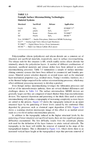
TABLE 3.3
Example Surface Micromachining Technologies
Material Systems
Structural Sacrificial Release Application
PolySi SiO 2 HF SUMMiT Ve
SiN polySi XeF 2 GLVe
Al Resist Plasma etch TI DMDe
SiC PolySi XeF 2 MUSICe
Note: SUMMiTe — Sandia Ultra-planar, Multi-level MEMS Technology
GLVe — Grating Light Valve (Silicon Light Machines)
TI DMDe — Digital Mirror Device (Texas Instruments)
MUSICe — Multi User Silicon Carbide (FLX micro)
Polycrystalline silicon (polysilicon) and silicon dioxide are a common set of
structural and sacrificial materials, respectively, used in surface micromachining.
The release etch for this situation is HF, which readily etches silicon dioxide but
minimally attacks the polysilicion layers. A number of different combinations of
structural, sacrificial materials and release etches have been utilized in surface
micromachining processes. Table 3.3 summarizes a sample of surface microma-
chining material systems that have been utilized in commercial and foundry pro-
cesses. Material system selection depends on several issues such as the structural
layer mechanical properties (e.g., residual stress, Young’s modulus, hardness, etc.)
or the thermal budget required in the surface micromachining processes, which may
affect additional processing necessary to develop a product.
Even though surface micromachining leverages the fabrication processes and
tool set of the microelectronics industry, there are several distinct differences and
challenges shown in Table 3.4. The surface micromachine MEMS devices are
generally larger and they are composed of much thicker films than microelectronic
devices. The repeated deposition and patterning of the thick films used in surface
micromachining will produce a topography of increasing complexity as more layers
are added to the process. Figure 3.9 shows the topography induced on an upper
structural layer by the patterning of lower levels caused by the conformal films
deposited by processes such as chemical vapor deposition (CVD). Figure 3.10
shows a scanning electron microscopic image of this effect in an inertial sensor
made in a two-level surface micromachine process.
In addition to the topography induced in the higher structural levels by the
patterning of lower structural and sacrificial layers, there are two significant process
difficulties encountered. The first difficulty results from the anisotropic plasma
etch used for the definition of the layer features to attain vertical sidewalls. The
topography in the layer will inhibit the removal of material in the steps of the
topographical features. This is illustrated in Figure 3.11, which shows there is an
increased vertical layer height at the topographical steps that prevents removal of
© 2006 by Taylor & Francis Group, LLC