
Page 65 - MEMS and Microstructures in Aerospace Applications
P. 65
Osiander / MEMS and microstructures in Aerospace applications DK3181_c003 Final Proof page 55 1.9.2005 8:59pm
MEMS Fabrication 55
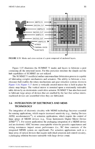
FIGURE 3.15 Masks and cross-section of a post composed of anchored layers.
Figure 3.15 illustrates the SUMMiT V masks and layers to fabricate a post
containing all the structural layers. For this particular structure the dimple and the
hub capabilities of SUMMiT are not utilized.
The SUMMiT V sacrificial surface micromachine fabrication process is capable
of fabricating complex mechanisms and actuators. The ability to fabricate a low-
clearance hub enables the rotary mechanisms and gear reduction systems shown in
Figure 3.16. Figure 3.17 shows a vertically erected mirror that is held in place by
elastic snap hinges. The vertical mirror is mounted upon a rotationally indexable
table driven by an electrostatic comb drive actuator. SUMMiT V has also been used
to fabricate large arrays of devices that are enabled by the fact that surface micro-
machined devices are assembled when they are fabricated.
3.6 INTEGRATION OF ELECTRONICS AND MEMS
TECHNOLOGY
The integration of electronic circuitry with MEMS technology becomes essential
for sensing applications, which require increased sensitivity (e.g., Analog Devices
32
ADXL accelerometers ), or actuation applications, which require the control of
large arrays of MEMS devices (e.g., Texas Instruments Digital Mirror Device
1 33
[DMD ] ). For sensor applications the packaging integration of a MEMS device
and an electronic ASIC becomes unacceptable when the parasitic capacitances and
wiring resistances impact sensor performance (i.e., RC time constants of the
integrated MEMS system are significant). For actuation applications such as a
large array of optical devices that require individual actuation and control circuitry,
a packaging solution becomes untenable with large device count.
© 2006 by Taylor & Francis Group, LLC