
Page 72 - Mechanical Engineers Reference Book
P. 72
Basic electrical technology 211 3
Therefore
R
__-
VO,,
-
V,, R + ~(wL l/&)
-
Using the complex conjugate and calculating the modulus of
the voltage ratio gives
R
(2.59)
[R2 + (WL - l/WC)2]”2
The phase angle
6 = -tan-’ (2.60)
The voltage ratio will have a maximum value of unity when the
frequency
(2.61)
Equation (2.61) defines the ‘resonance’ condition at which
the inductive and capacitive reactances are equal and self-
cancelling. The resonant frequency is usually denoted w0 and
it is the frequency at which the power transferred through the
circuit 11s maximum. At any other frequency above or below w0
the power transferred is reduced.
The impedance of the circuit is given by
-
Z R + j(XL - Xc) (2.62)
At the resonant frequency the total reactance is zero and the
circuit behaves as if only the resistive element were present.
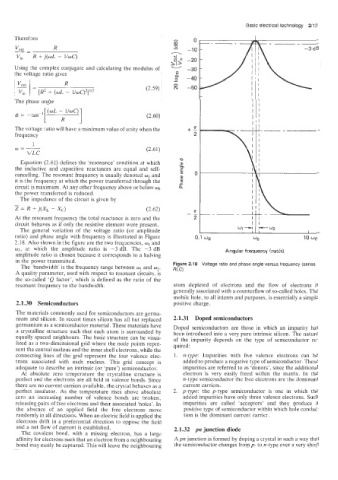
The general variation of the voltage ratio (or amplitude
ratio) and phase angle with frequency is illustrated in Figure 0.1 wo 10 wo
2.18. A.lso shown in the figure are the two frequencies, w1 and
w2, at which the amplitude ratio is -3 dB. The -3 dB Angular frequency (rad/s)
amplitude ratio is chosen because it corresponds to a halving
in the power transmitted. Figure 2.18 Voltage ratio and phase angle versus frequency (series
The ‘,bandwidth’ is the frequency range between o1 and w2. RLC)
A quality parameter, used with respect to resonant circuits, is
the so-called ‘Q factor’, which is defined as the ratio of the
resonant frequency to the bandwidth. atom depleted of electrons and the flow of electrons is
generally associated with a counterflow of so-called holes. The
mobile hole, to all intents and purposes, is essentially a simple
2.1.30 Semiconductors positive charge.
The materials commonly used for semiconductors are germa-
nium and silicon. In recent times silicon has all but replaced 2.1.31 Doped semiconductors
germanium as a semiconductor material. These materials have
a crystalline structure such that each atom is surrounded by Doped semiconductors are those in which an impurity has
been introduced into a very pure intrinsic silicon. The nature
equally spaced neighbours. The basic structure can be visua- of the impurity depends on the type of semiconductor re-
lized as a two-dimensional grid where the node points repre- quired:
sent the central nucleus and the inner shell electrons, while the
connecting lines of the grid represent the four valence elec- 1. n-type: Impurities with five valence electrons can be
trons associated with each nucleus. This grid concept is added to produce a negative type of semiconductor. These
adequate to describe an intrinsic (or ‘pure’) semiconductor. impurities are referred to as ‘donors’, since the additional
At absolute zero temperature the crystalline structure is electron is very easily freed within the matrix. In the
perfect and the electrons are all held in valence bonds. Since n-type semiconductor the free electrons are the dominant
there are no current carriers available, the crystal behaves as a current carriers.
perfect insulator. As the temperature rises above absolute 2. p-type: the p-type semiconductor is one in which the
zero an increasing number of valence bonds are broken, added impurities have only three valence electrons. Such
releasing pairs of free electrons and their associated ‘holes’. In impurities are called ‘acceptors’ and they produce a
the absence of an applied fieid the free electrons move positive type of semiconductor within which hole conduc-
randomly in all directions. When an electric field is applied the tion is the dominant current carrier.
electrons drift in a preferential direction to oppose the field
and a net flow of current is established. 2.1.32 pn junction diode
The covalent bond, with a missing electron, has a large
affinity for electrons such that an electron from a neighbouring A pn junction is formed by doping a crystal in such a w2y that
bond may easily be captured. This will leave the neighbouring the semiconductor changes from p- to n-type over a very short