
Page 73 - Mechanical Engineers Reference Book
P. 73
2/14 Electrical and electronics principles
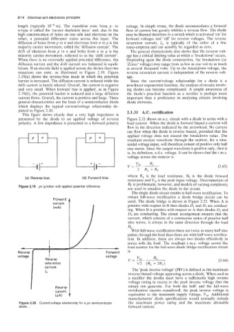
length (typically m). The transition zone from p- to voltage. In simple terms, the diode accommodates a forward
n-type is called the ‘carrier depletion layer’ and, due to the flow of current but greatly inhibits a reverse flow. The diode
high concentration of holes on one side and electrons on the may be likened therefore to a switch which is activated ‘on’ for
other, a potential difference exists across this layer. The forward voltages and ‘off‘ for reverse voltages. The reverse
diffusion of holes from p to n and electrons from n to p is the saturation current, Is, is typically of the order of a few
majority carrier movement, called the ‘diffusion current’. The nano-amperes and can sensibly be regarded as zero.
drift of electrons from p to n and holes from n to p is the The general characteristic also shows that the reverse volt-
minority carrier movement. referred to as the ‘drift current’. age has a critical limiting value at which a ‘breakdown’ occurs.
When there is no externally applied potential difference, the Depending upon the diode construction, the breakdown (or
diffusion current and the drift current are balanced in equili- ‘Zener’ voltage) may range from as low as one volt to as much
brium. If an electric field is applied across the device then two as several thousand volts. Up to the breakdown voltage, the
situations can exist, as illustrated in Figure 2.19. Figure reverse saturation current is independent of the reverse volt-
2.19(a) shows the reverse-bias mode in which the potential age.
barrier is increased. The diffusion current is reduced while the Since the currentholtage relationship for a diode is a
drift current is barely altered. Overall, the current is negative non-linear exponential function, the analysis of circuits involv-
and very small. When forward bias is applied, as in Figure ing diodes can become complicated. A simple awareness of
2.19(b), the potential barrier is reduced and a large diffusion the diode’s practical function as a rectifier is perhaps more
current flows. Overall, the current is positive and large. These important than a proficiency in analysing circuits involving
general characteristics are the basis of a semiconductor diode diode elements.
which displays the typical currentholtage relationship de-
picted in Figure 2.20. 2.1.33 A.C. rectification
This figure shows clearly that a very high impedance is
presented by the diode to an applied voltage of reverse Figure 2.21 shows an a.c. circuit with a diode in series with a
polarity. A low impedance is presented to a forward polarity load resistor. When the diode is forward biased a current will
flow in the direction indicated by the arrowhead. No current
can flow when the diode is reverse biased, provided that the
applied voltage does not exceed the breakdown value. The
resultant current waveform through the resistor, for a sinu-
soidal voltage input, will therefore consist of positive only half
sine waves. Since the output waveform is positive only, then it
is, by definition, a d.c. voltage. It can be shown that the r.m.s.
voltage across the resistor is
(2.63)
(a) Reverse bias (b) Forward bias where RL is the load resistance, RF is the diode forward
resistance and V, is the peak input voltage. Determination of
Figure 2.19 pn junction with applied potential difference RF is problematic, however, and models of varying complexity
are used to simulate the diode in the circuit.
The single-diode circuit results in half-wave rectification. To
obtain full-wave rectification a diode bridge circuit can be
Forward
current used. The diode bridge is shown in Figure 2.22. When A is
positive with respect to B then diodes D1 and D3 are conduct-
( mA)
ing. When B is positive with respect to A then diodes D2 and
04 are conducting. The circuit arrangement ensures that the
current, which consists of a continuous series of positive half
sine waves, is always in the same direction through the load
RL.
With full-wave rectification there are twice as many half sine
pulses through the load than there are with half-wave rectifica-
tion. In addition, there are always two diodes effectively in
series with the load. The resultant r.m.s. voltage across the
load resistor for the full-wave diode bridge rectification circuit
Reverse t Forward is
voltage voltage
Reverse (2.64)
saturation
current
Is The ‘peak inverse voltage’ (PIV) is defined as the maximum
reverse-biased voltage appearing across a diode. When used as
a rectifier the diodes must have a sufficiently high reverse
voltage rating in excess to the peak inverse voltage that the
Reverse circuit can generate. For both the half- and the full-wave
current rectification circuits considered, the peak inverse voltage is
I (PA) equivalent to the maximum supply voltage, V,. Additional
manufacturers’ diode specifications would normally include
Figure 2.20 Currentivoltage relationship for a pn semiconductor the maximum power rating and the maximum allowable
diode forward current.