
Page 156 - Mechatronics for Safety, Security and Dependability in a New Era
P. 156
Ch29-I044963.fm Page 140 Tuesday, August 1, 2006 3:05 PM
Ch29-I044963.fm
140
140 Page 140 Tuesday, August 1, 2006 3:05 PM
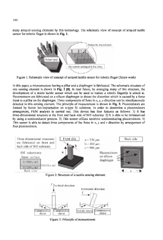
many arrayed sensing elements by this technology. The schematic view of concept of arrayed tactile
sensor for robotic finger is shown in Fig. 1.
The sensors arranged in the array
Figure 1: Schematic view of concept of arrayed tactile sensor for robotic finger (future work)
In this paper, a microstructure having a pillar and a diaphragm is fabricated. The schematic structure of
one sensing element is shown in Fig. 2 [8]. In near future, by arranging many of this structure, the
development of a micro tactile sensor which can be used to realize a robot's fingertip is aimed at.
Piezoresistors are fabricated on a silicon diaphragm to detect the distortion which is caused by a force
input to a pillar on the diaphragm. Three components of force in x, y, z direction can be simultaneously
detected in this sensing element. The principle of measurement is shown in Fig. 3. Piezoresistors are
formed by boron ion-implantation on n-type Si substrate. In order to determine a piezoresistors
arrangement, FEM analysis is carried out. This device has four features as follows: 1) It has
three-dimensional structure at the front and back side of SOI substrate. 2) Tt is able to be miniaturized
by using a semiconductor process. 3) This sensor utilizes sensitive semiconducting piezoresistors. 4)
This sensor is able to detect three components of the force in x, y and z direction by arrangement of
four piezoresistors.
Three dimensional structures F r o n t s i d e I a = 220um Back side
are fabricated on front and ^ A , b = 400 urn
back side of SOI substrate.
c = 900 um
SOI substrate Piezoresistors
Upper surface on silicon
diaphragm
Si(500/im)
Si(100y m) Sl °
Back side
Figure 2: Structure of a tactile sensing element
f
IVertic ; direction
Vertical
Horizontal direction
f
1 I
Compressive Compressive Tensile stress Compressive
stress stress stress
Figure 3: Principle of measurement