
Page 158 - Mechatronics for Safety, Security and Dependability in a New Era
P. 158
Ch29-I044963.fm Page 142 Tuesday, August 1, 2006 3:05 PM
Ch29-I044963.fm
142
142 Page 142 Tuesday, August 1, 2006 3:05 PM
SOI wafer Etch Si by KOH Drive Boron ion by annealing
Oxidize both sides
photoresist
Deep RTE of Si for pillar
Oxidize both sides Spin-coat photoresist Evaporate aluminum
Spin-coat photoresist Pattern photoresist Spin-coat and pattern resist
and pattern it B
Etch SiO 2 by CHF3 Etch aluminum
Implant Boron ion by H 3 PO 4
plasma gas
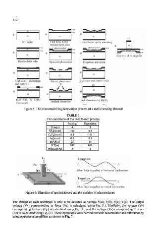
Figure 5: The micromachining fabrication process of a tactile sensing element
TABLE 1
The conditions of the used Bosch process
Etching Deposition
Time[s] 4 3
SF 6[sccm] 100 0.5
C 4F 8[sccm] 0.5 100
Ar[sccm] 0.5 0.5
BIAS[w] 25 15
ICP[w] 500 600
Pressure [Pa] 5 5
Tension
nsion
•
When force is applied in horizontal (x) direction
When force is applied in vertical (z) direction
Figure 6: Direction of applied forces and the position of piezoresistors
The change of each resistance is able to be detected as voltage V(a), V(b), V(c), V(d). The output
voltage (Vx) corresponding to force (Fx) is calculated using Eq. (1). Similarly, the voltage (Vy)
corresponding to force (Fy) is calculated using Eq. (2), and the voltage (Vz) corresponding to force
(Fz) is calculated using Eq. (3). These operations were carried out with accumulator and subtractor by
using operational amplifiers as shown in Fig. 7.