
Page 157 - Mechatronics for Safety, Security and Dependability in a New Era
P. 157
Ch29-I044963.fm Page 141 Tuesday, August 1, 2006 3:05 PM
Page 141
1, 2006
3:05 PM
Tuesday, August
Ch29-I044963.fm
141
141
FEM (FINITE ELEMENT METHOD) ANALYSIS
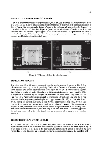
In order to determine the position of piezoresistor, FEM analysis is carried out. When the force of 10
gf is applied to the pillar tip of the sensing element, the results of distortion of a diaphragm is shown in
Fig. 4. Figure 4 (a) shows the distribution of strain in the horizontal direction, when the force of lOgf
is applied in the vertical direction. Figure 4 (b) shows the distribution of strain in the horizontal
direction, when the force of 10 gf is applied in the horizontal direction. It is proved that the strain is
maximal at the edge of the diaphragm. Therefore, the four piezoresistors are designed to be located as
close as possible to the edge of the diaphragm.
ANSYS ANSYS
STEP=1
fcBsSM
SHX =.40DE-03 I
I Pressure is applied
in vertical direction Pressure is applied in
c ) K horizontal direction )
Co mpressive
Compressil-e ® r Tensile Compressive
stress stress stress stress
Strain of horizontal Strain of horizontal
Back side direction is shown Back side direction is shown
i
— - •
(a) (b)
Figure 4: FEM result of distortion of a diaphragm.
FABRICATION PROCESS
The micro-machining fabrication process of a tactile sensing element is shown in Fig. 5. The
microstructure detecting a force is practically fabricated as follows: a SOI wafer is prepared,
which consists of a silicon layer (called as active layer) of 100 urn, a silicon dioxide layer of
lum (called as box layer), and a silicon layer of 500 u.m (called as support layer) (see Fig. 5®).
A diaphragm is fabricated by anisotropic wet etching of the active layer using KOH solution
(see Fig. 5©). Piezoresistors are produced by implanting p-type boron ions into the n-type
silicon of the diaphragm using an ion implantation apparatus (see Fig. 5®). A pillar is fabricated
by dry etching the support layer using a deep ICP-RIE apparatus (see Fig. 5©). ICP-RIE was
performed by Bosch process and their condition are shown in Table 1 [9J. Aluminum is
evaporated and patterned for electrodes, which connect the piezoresistors to the bonding pads.
The wafer is diced to square chips, and each chip is set on a print board. The bonding pads of
the chip are connected to the print board pads by aluminum wires using a wire bonding
apparatus.
THE DESIGN OF EVALUATION CIRCUIT
The direction of applied forces and the position of piezoresistors are shown in Fig. 6. When force is
applied to the pillar in the x direction, the distortion appears as shown in the upper right of Fig. 6.
When force is applied to the pillar in the z direction, the distortion will appear as shown in the lower
right of Fig. 6. This distortion can be detected by four piezoresistors arranged as shown in Fig. 6 [8].