
Page 256 - A Practical Guide from Design Planning to Manufacturing
P. 256
228 Chapter Seven
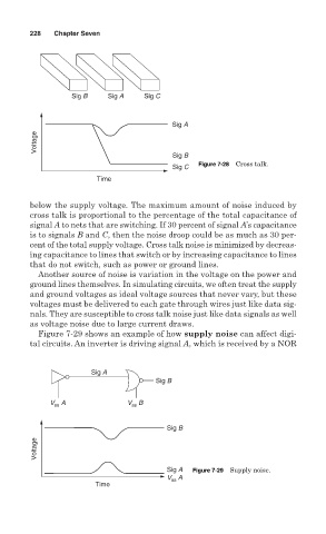
Sig B Sig A Sig C
Sig A
Voltage
Sig B
Figure 7-28 Cross talk.
Sig C
Time
below the supply voltage. The maximum amount of noise induced by
cross talk is proportional to the percentage of the total capacitance of
signal A to nets that are switching. If 30 percent of signal A’s capacitance
is to signals B and C, then the noise droop could be as much as 30 per-
cent of the total supply voltage. Cross talk noise is minimized by decreas-
ing capacitance to lines that switch or by increasing capacitance to lines
that do not switch, such as power or ground lines.
Another source of noise is variation in the voltage on the power and
ground lines themselves. In simulating circuits, we often treat the supply
and ground voltages as ideal voltage sources that never vary, but these
voltages must be delivered to each gate through wires just like data sig-
nals. They are susceptible to cross talk noise just like data signals as well
as voltage noise due to large current draws.
Figure 7-29 shows an example of how supply noise can affect digi-
tal circuits. An inverter is driving signal A, which is received by a NOR
Sig A
Sig B
V ss A V ss B
Sig B
Voltage
Sig A Figure 7-29 Supply noise.
V ss A
Time