
Page 257 - A Practical Guide from Design Planning to Manufacturing
P. 257
Circuit Design 229
gate some distance away. The inverter has no noise on its input, and
there is no cross talk affecting signal A, but a large current draw by
another gate near the inverter causes the ground voltage at the inverter
(V A) to be pulled up. The inverter continues to drive its output to
ss
ground, but now its ground voltage is higher than the ground voltage
at the receiver. The NOR gate will begin to switch low because its input
is now at a higher voltage than the NOR gate’s local ground line. Providing
very low resistance paths for the supply and ground voltages to all gates
minimizes supply noise.
Paths with very little timing margin cause another type of noise. When
inputs to sequentials switch just before or after the sequential closes, the
storage node of the sequential will be disturbed. Even with all other sources
of noise eliminated, just having very little timing margin can put nodes
at intermediate voltages between the supply and ground.
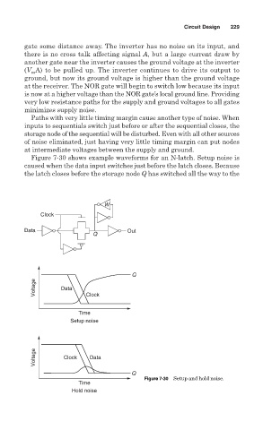
Figure 7-30 shows example waveforms for an N-latch. Setup noise is
caused when the data input switches just before the latch closes. Because
the latch closes before the storage node Q has switched all the way to the
W
Clock
Data Out
Q
Q
Voltage Data Clock
Time
Setup noise
Voltage Clock Data
Q
Figure 7-30 Setup and hold noise.
Time
Hold noise