
Page 234 - Microsensors, MEMS and Smart Devices - Gardner Varadhan and Awadelkarim
P. 234
214 MICROSTEREOLITHOGRAPHY FOR MEMS
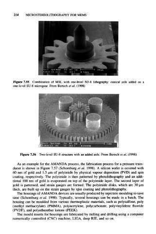
Figure 7.55 Combination of MSL with one-level SU-8 lithography: conical axle added on a
one-level SU-8 microgear. From Bertsch et al. (1998)
Figure 7.56 Two-level SU-8 structure with an added axle. From Bertsch et al. (1998)
As an example for the AMANDA process, the fabrication process for a pressure trans-
ducer is shown in Figure 7.57 (Schomburg et al. 1998). A silicon wafer is covered with
60 nm of gold and 1.5 urn of polyimide by physical vapour deposition (PVD) and spin
coating, respectively. The polyimide is then patterned by photolithography and an add-
tional 100 nm of gold is evaporated on top of the polyimide layer. The second layer of
gold is patterned, and strain gauges are formed. The polyimide disks, which are 30 urn
thick, are built up on the strain gauges by spin coating and photolithography.
The housings of AMANDA devices are usually produced by injection moulding to save
time (Schomburg et al. 1998). Typically, several housings can be made in a batch. The
housing can be moulded from various thermoplastic materials, such as polysulfone, poly
(methyl methacrylate) (PMMA), polyacetylene, polycarbonate, polyvinylidene fluoride
(PVDF), and polyetherether ketone (PEEK).
The mould inserts for housings are fabricated by milling and drilling using a computer
numerically controlled (CNC) machine, LIGA, deep RIE, and so on.