
Page 230 - Microsensors, MEMS and Smart Devices - Gardner Varadhan and Awadelkarim
P. 230
210 MICROSTEREOLITHOGRAPHY FOR MEMS
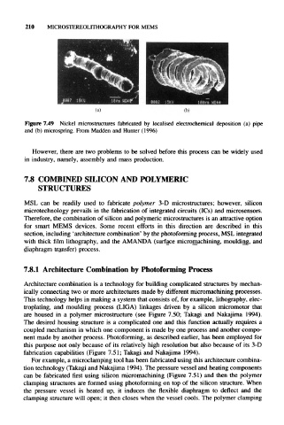
Figure 7.49 Nickel microstructures fabricated by localised electrochemical deposition (a) pipe
and (b) microspring. From Madden and Hunter (1996)
However, there are two problems to be solved before this process can be widely used
in industry, namely, assembly and mass production.
7.8 COMBINED SILICON AND POLYMERIC
STRUCTURES
MSL can be readily used to fabricate polymer 3-D microstructures; however, silicon
microtechnology prevails in the fabrication of integrated circuits (ICs) and microsensors.
Therefore, the combination of silicon and polymeric microstructures is an attractive option
for smart MEMS devices. Some recent efforts in this direction are described in this
section, including 'architecture combination' by the photoforming process, MSL integrated
with thick film lithography, and the AMANDA (surface micromachining, moulding, and
diaphragm transfer) process.
7.8.1 Architecture Combination by Photoforming Process
Architecture combination is a technology for building complicated structures by mechan-
ically connecting two or more architectures made by different micromachining processes.
This technology helps in making a system that consists of, for example, lithography, elec-
troplating, and moulding process (LIGA) linkages driven by a silicon micromotor that
are housed in a polymer microstructure (see Figure 7.50; Takagi and Nakajima 1994).
The desired housing structure is a complicated one and this function actually requires a
coupled mechanism in which one component is made by one process and another compo-
nent made by another process. Photoforming, as described earlier, has been employed for
this purpose not only because of its relatively high resolution but also because of its 3-D
fabrication capabilities (Figure 7.51; Takagi and Nakajima 1994).
For example, a microclamping tool has been fabricated using this architecture combina-
tion technology (Takagi and Nakajima 1994). The pressure vessel and heating components
can be fabricated first using silicon micromachining (Figure 7.51) and then the polymer
clamping structures are formed using photoforming on top of the silicon structure. When
the pressure vessel is heated up, it induces the flexible diaphragm to deflect and the
clamping structure will open; it then closes when the vessel cools. The polymer clamping