
Page 227 - Microsensors, MEMS and Smart Devices - Gardner Varadhan and Awadelkarim
P. 227
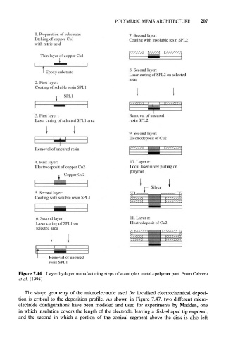
POLYMERIC MEMS ARCHITECTURE      207

            1. Preparation  of  substrate:       7. Second layer:
            Etching of copper  Cul               Coating with insoluble resin SPL2
            with nitric acid

              Thin layer of copper Cu 1


                                                 8. Second layer:
               I  Epoxy substrate
                                                 Laser curing of SPL2 on selected
                                                 area
            2. First layer:
            Coating of soluble resin SPL1
                        SPL1


            3. First layer:                      Removal of uncured
            Laser curing of selected SPL1 area   resin SPL2

                                                 9. Second  layer:
                                                 Electrodeposit of Cu2

            Removal of uncured resin

            4. First layer:                      10. Layer n:
            Electrodeposit of copper Cu2         Local laser silver plating on
                                                 polymer
                        Copper Cu2


            5. Second layer:
            Coating with soluble resin SPL1


             6. Second layer:                    11. Layer n:
             Laser curing of SPL1 on             Electrodeposit of Cu2
             selected area


                  Removal of uncured
                  resin SPL1
     Figure  7.44 Layer-by-layer manufacturing  steps of a complex  metal-polymer  part. From  Cabrera
     et al. (1998)

       The  shape  geometry  of  the  microelectrode  used for  localised  electrochemical  deposi-
     tion  is  critical  to  the  deposition  profile. As  shown in  Figure  7.47,  two  different  micro-
     electrode  configurations have  been  modeled  and  used  for  experiments  by  Madden,  one
     in  which insulation  covers  the  length of the electrode, leaving a disk-shaped  tip  exposed,
     and  the  second  in  which  a  portion  of  the  conical  segment  above  the  disk  is  also  left