
Page 224 - Microsensors, MEMS and Smart Devices - Gardner Varadhan and Awadelkarim
P. 224
204 MICROSTEREOLITHOGRAPHY FOR MEMS
(a) Electrolyte
Blanket-
deposited
2nd material
Selectivity-
Substrate
material
Sacrificial
Structural material (support)
material
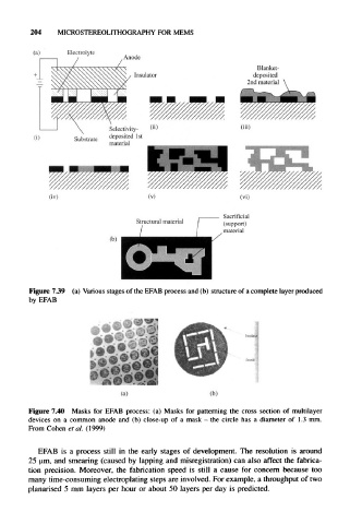
Figure 739 (a) Various stages of the EFAB process and (b) structure of a complete layer produced
by EFAB
(a) (b)
Figure 7.40 Masks for EFAB process: (a) Masks for patterning the cross section of multilayer
devices on a common anode and (b) close-up of a mask - the circle has a diameter of 1.3 mm.
From Cohen et al. (1999)
EFAB is a process still in the early stages of development. The resolution is around
25 um, and smearing (caused by lapping and misregistration) can also affect the fabrica-
tion precision. Moreover, the fabrication speed is still a cause for concern because too
many time-consuming electroplating steps are involved. For example, a throughput of two
planarised 5 mm layers per hour or about 50 layers per day is predicted.