
Page 226 - Microsensors, MEMS and Smart Devices - Gardner Varadhan and Awadelkarim
P. 226
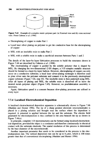
206    MICROSTEREOLITHOGRAPHY FOR MEMS


                                                             Metal
                                                             (Part  1)


      Figure 7.43  Example of a complex  metal-polymer  part: (a) External view and (b) cross  sectional
      view. From  Cabrera  et al. (1998)

      •  Electroplating  of copper  to make Part 1

      •  Local  laser  silver  plating on polymer  to get the conductive  base for the  electroplating
        of  copper
      •  MSL with an insoluble resin to make Part 2

      •  MSL with a soluble  resin to make a sacrificial structure between  Parts  1 and 2

      The  details  of  the  layer-by-layer fabrication  processes  to  build  the  structures shown in
      Figure  7.44  are described  by Cabrera  et al.  (1998).
        The  electroplating  of  copper  is  guided  by  the  soluble  polymer  that  is  shaped  by
      MSL.  By changing  the  two-dimensional  (2-D)  shapes, a  3-D complex  metallic  structure
      should  be formed in a layer-by-layer  fashion.  However,  electroplating  of copper  can only
      occur  on  a  conductive  substrate;  a  local  laser  silver-plating  technique  is  therefore  used
      to  plate  silver onto  the  polymer  substrate  and  connect  it  to  the  previously  electroplated
      copper  substrate  (Figure  7.44,  step  10). The insoluble resin  is then patterned  using MSL.
      After  all  layers  of  plating  and  MSL,  the  soluble  resin  is  dissolved  off  to  leave  the
      desired  metal-polymer  object  (Figure  7.45).  However,  no  postfabrication  assembly  is
      necessary.
        Again,  fabrication  speed  is  a  concern  because  slow-plating  processes  are  utilised  in
     every  layer.


     7.7.4  Localised  Electrochemical  Deposition

     A  localised  electrochemical  deposition  apparatus is  schematically shown in  Figure  7.46
     (Madden  and  Hunter  1996).  The  tip  of  a  sharp  pointed  electrode  (microelectrode)  is
     placed  in  a  plating  solution  and  brought  near  the  surface  where  the  deposition  is
     required.  A  potential  is  applied  between  the  tip  and  the  substrate.  The  electric  field
     generated  for  electrodeposition  is thus confined  to  the  area  beneath  the  tip  as  shown  in
     Figure  7.46(a).
        In principle,  complete  3-D microstructures  can be formed using localised  electrochem-
     ical deposition,  provided  the object is a conductor and therefore continuously in  electrical
     contact  with the  substrate  electrode.  The  spatial  resolution of  this  process  is determined
     by  the  base  diameter of  the  microelectrode.
        Another  important  parameter  that  needs  to  be  considered  in  the  process  is  the  elec-
     trodeposition  rate.  The  vertical  deposition  rate  can be  up  to  6 um/s, which is  100 times
     greater  than that of conventional  electroplating  (Madden  and Hunter  1996).