
Page 223 - Microsensors, MEMS and Smart Devices - Gardner Varadhan and Awadelkarim
P. 223
203
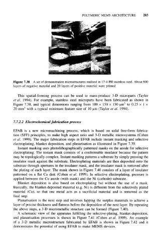
Figure 7.38 A set of demonstration microstructures realised in 17–4 PH stainless steel. About 600
layers of negative material and 20 layers of positive material were printed
This spatial-forming process can be used to mass-produce 3-D microparts (Taylor
et al. 1994). For example, stainless steel microparts have been fabricated as shown in
Figure 7.38, and typical dimensions ranging from 100 x 150 x 150 um 3 to 0.25 x 1 x
20 mm 3 with a typical minimum feature size of 10 urn (Taylor et al. 1994).
7.7.2.2 Electrochemical fabrication process
EFAB is a new micromachining process, which is based on solid free-form fabrica-
tion (SFF) principles, to make high aspect ratio and 3-D metallic microsystems (Cohen
et al. 1999). The major fabrication steps in EFAB include instant masking and selective
electroplating, blanket deposition, and planarisation as illustrated in Figure 7.39.
Instant masking uses photolithographically patterned masks on the anode for selective
electroplating. The instant mask consists of a conformable insulator because the pattern
may be topologically complex. Instant masking patterns a substrate by simply pressing the
insulator mask against the substrate. Electroplating materials are then deposited onto the
substrate through apertures in the insulator mask, and the insulator mask is removed after
the plating of each layer. The mask shown in Figure 7.40 consists of a layer of insulator
patterned on a flat Cu disk (Cohen et al. 1999). In selective electroplating, pressure is
applied between the Cu anode (with mask) and the Ni (cathode) substrate.
Blanket deposition is also based on electroplating but without the use of a mask.
Basically, the blanket-deposited material (e.g. Ni) is different from the selectively plated
material (Cu), so that one metal acts as a sacrificial material and is removed as the
final step.
Planarisation is the next step and involves lapping the surplus materials to achieve a
layer of precise thickness and flatness before the deposition of the next layer. By repeating
the above steps, a 3-D micrometallic structure can be formed (Figure 7.40).
A schematic view of the apparatus fulfilling the selective-plating, blanket-deposition,
and planarisation processes is shown in Figure 7.41 (Cohen et al. 1999). An example
of a 3-D metallic microstructure fabricated by EFAB is shown in Figure 7.42 and it
demonstrates the potential of using EFAB to make MEMS devices.