
Page 229 - Microsensors, MEMS and Smart Devices - Gardner Varadhan and Awadelkarim
P. 229
POLYMERIC MEMS ARCHITECTURE 209
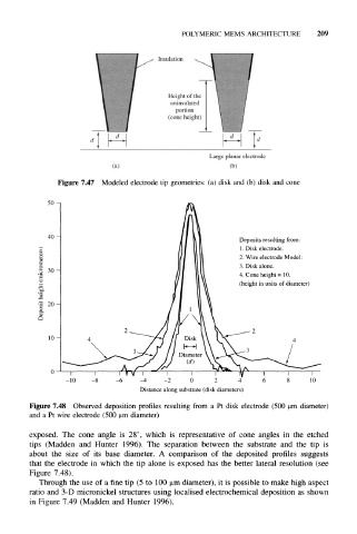
Figure 7.47 Modeled electrode tip geometries: (a) disk and (b) disk and cone
50 -i
Deposits resulting from:
1. Disk electrode.
2. Wire electrode Model:
3. Disk alone.
4. Cone height = 10.
(height in units of diameter)
-10 -4 -2 0
Distance along substrate (disk diameters)
Figure 7.48 Observed deposition profiles resulting from a Pt disk electrode (500 diameter)
and a Pt wire electrode (500 urn diameter)
exposed. The cone angle is 28°, which is representative of cone angles in the etched
tips (Madden and Hunter 1996). The separation between the substrate and the tip is
about the size of its base diameter. A comparison of the deposited profiles suggests
that the electrode in which the tip alone is exposed has the better lateral resolution (see
Figure 7.48).
Through the use of a fine tip (5 to 100 um diameter), it is possible to make high aspect
ratio and 3-D micronickel structures using localised electrochemical deposition as shown
in Figure 7.49 (Madden and Hunter 1996).