
Page 256 - Book Hosokawa Nanoparticle Technology Handbook
P. 256
4.5 STRUCTURE CONTROL OF NANOPARTICLE COLLECTIVES BY SINTERING AND BONDING FUNDAMENTALS
(a) Coherent boundary (b) Semicoherent boundary
(c) Incoherent boundary (d) Pseudo-coherent boundary
Figure 4.5.14
Types of dissimilar materials interfaces.
a degree of lattice mismatching. In general, it is called
a large mismatching when the mismatching is larger
than 4 5% and a small one when the mismatching is
smaller than 4 5%. The Nb–Al O system belongs to
2
3
the latter one.
A dislocation, which is one of lattice defects, is
introduced to relieve a lattice mismatching at the
interface. When the lattice mismatching between
metal and ceramics is small, a coherent boundary
(see Fig. 4.5.14(a)) is formed by a uniform strain of
crystal itself [10]. A condition to form such a coher-
ent boundary depends on a degree of mismatching
and a thickness of crystal. When the thickness of
crystal exceeds a critical one, the dislocations (see Figure 4.5.15
Fig. 4.5.14(b)) are introduced to relieve an increased SEM observation at the interface between -SiC and Cu.
strain and a semi-coherent boundary is formed
which is shown in Fig. 4.5.14(b). As shown in
Fig. 4.5.14(c), an incoherent boundary is formed
when an interaction does not exist at the interface.
This state represents that two kinds of crystal contact
only at the interface. When two crystals are joined at
the interface, atomic interaction takes place at the
interface and atomic displacements occur at near
interfaces shown in Fig. 4.5.14(d). Accordingly, the
coherent region takes the structure that is divided by
geometric miss-fit dislocation. The miss-fit disloca-
tion is formed in the crystal whose Young’s modulus
is smaller than the others’.
An oxide ceramics is superior in a thermodynami-
cal stability to a carbide and a nitride ceramics in gen-
eral. Accordingly, a steep interface is formed in
metal/oxide ceramics systems as shown in Fig. 4.5.14.
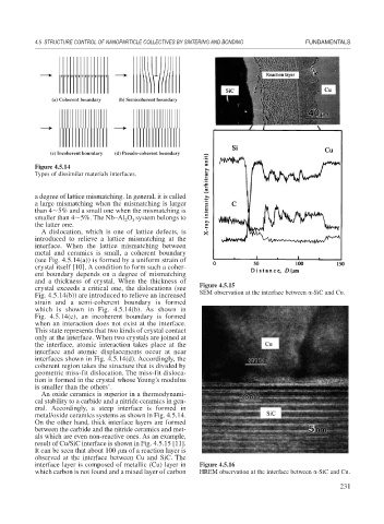
On the other hand, thick interface layers are formed
between the carbide and the nitride ceramics and met-
als which are even non-reactive ones. As an example,
result of Cu/SiC interface is shown in Fig. 4.5.15 [11].
It can be seen that about 100 m of a reaction layer is
observed at the interface between Cu and SiC. The
interface layer is composed of metallic (Cu) layer in Figure 4.5.16
which carbon is not found and a mixed layer of carbon HREM observation at the interface between -SiC and Cu.
231