
Page 257 - Book Hosokawa Nanoparticle Technology Handbook
P. 257
FUNDAMENTALS CH. 4 CONTROL OF NANOSTRUCTURE OF MATERIALS
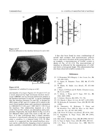
Figure 4.5.17
Electron diffraction at the interface between Cu and -SiC.
It has also been found in some combinations of
metals and ceramics that nanostructure reflects
macro- and micro-structure at the joined interface. As
an example, a macrostructure of Cu/SiC system is
shown in Fig. 4.5.18 [13]. The macrostructure of
interface is reflected by the nanostructure of -SiC
and shows a hexagonal shape. This phenomenon has
also been observed in In/Ge system [14].
References
[1] G. Economos, W.D. Kingery: J. Am. Ceram. Soc., 36,
403–409 (1963).
[2] K. Ogino, H. Taimatsu: Trans. JIM, 46, 871–876
(1982).
[3] W. Mader, M. Ruhle: Acta Metall., 37, 853–866
Figure 4.5.18 (1989).
Appearance of solidified Cu drop on -SiC. [4] J. Mayer, C.P. Flynn and M. Ruhle: Ultramicroscopy,
33, 51–61 (1990).
and metallic (Cu) layer. Figures 4.5.16 and 4.5.17 are [5] Y. Ishida, J. Wang and T. Suga: ISIJ Int., 30,
a result observed by high resolution electron micro-
scope (HREM) and an electron diffraction pattern at 1041–1045 (1990).
the interface between Cu and SiC. It can be concluded [6] Y. Ikuhara: Materia, 34 (1995), 751–756.
that the interface between Cu and SiC is formed by [7] F.S. Ohuchi: J. Mater. Sci. Lett., 8, 1427–1429 (1989).
(001) plane of SiC and (111) plane of Cu which is the [8] M. Kohyama, R. Yamamoto: Trans. JIM, 29, 893–901
most closed packed plane and a preferred orientation (1990).
is {100}SiC//{111}Cu and 100 SiC// 110 Cu at [9] R. Yamamoto, M. Kohyama, Y. Ebata and
the interface. This relationship depends on a thin M. Kinoshita: Proc. MRS Int. Meet. on Adv. Mater.
oxide film on SiC surface, an atmosphere and a tem- (Mat. Res. Soc.), 8, 183–188 (1989).
perature. Especially, the result shown in Fig. 4.5.16 is [10] G.B. Olson, M. Cohen: Acta Metall., 27 (1979), 1907.
not obtained when oxide film exists at the SiC sur- [11] K. Suganuma, K. Nogi: Trans. JIM, 59 (1995),
face. It is also well-known that a joined interface
structure is significantly affected by a sintering agent 1292–1298.
when a ceramics is a sintered body [12]. In other [12] M.E. Brito, Y. Hirotsu: Trans. JIM, 29 (1990), 910–917.
words, it is suggested that the joined interface struc- [13] K. Nogi, K. Ogino: Trans. JIM, 29 (1988), 805–811.
ture can be controlled by changing a kind of sintering [14] A.A. Berg: J. Electrochem. Soc., 110, 908–914
agent, quantity, a temperature, and an atmosphere. (1963).
232