
Page 345 - Power Electronics Handbook
P. 345
Design of inverter circuits 335
THc
I_
a=-
r-
0
‘4 LE TI_. TI 7- .+,L
6
2 6+t
N
0
2 1 2 l 2 l 2 l 2 1 2
3 4 5 4 3 6 7 8 7 6 3
(b)
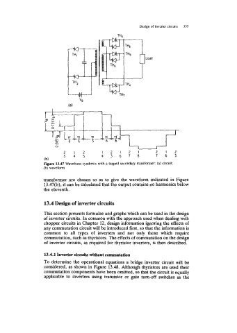
Figure 13.47 Waveform synthesis with a tapped secondary transformer: (a) circuit;
(b) waveform
transformer are chosen so as to give the waveform indicated in Figure
13.47(b), it can be calculated that the output contains no harmonics below
the eleventh.
13.4 Design of inverter circuits
This section presents formulae and graphs which can be used in the design
of inverter circuits. In common with the approach used when dealing with
chopper circuits in Chapter 12, design information ignoring the effects of
any commutation circuit will be introduced first, so that the information is
common to all types of inverters and not only those which require
commutation, such as thyristors. The effects of commutation on the design
of inverter circuits, as required for thyristor inverters, is then described.
13.4.1 Inverter circuits without commutation
To determine the operational equations a bridge inverter circuit will be
considered, as shown in Figure 13.48. Although thyristors are used their
commutation components have been omitted, so that the circuit is equally
applicable to inverters using transistor or gate turn-off switches as the