
Page 347 - Power Electronics Handbook
P. 347
Design of inverter circuits 337
control semiconductors. The operation of this circuit has already been
briefly introduced and may be readily followed by reference to the circuit
waveforms shown in Figure 13.49. As expected, the supply current shows
periods of regeneration, which is a maximum when there is no zero dwell
period in the load voltage waveform. It also increases as the power factor
of the load decreases, and for a purely inductive load the current shows
equal areas above and below the zero line, indicating that no net power is
taken from the supply.
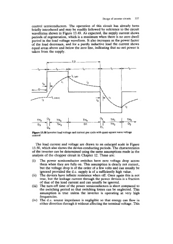
Figure 13.50 Inverter load voltage and current per cycle with quasi-square wave voltage
control
The load current and voltage are drawn to an enlarged scale in Figure
13.50, which also shows the device-conducting periods. The characteristics
of the inverter can be determined using the same assumptions made in the
analysis of the chopper circuit in Chapter 12. These are:
(i) The power semiconductor switches have zero voltage drop across
them when they are fully on. This assumption is clearly not correct,
but the voltage drop is of the order of a few volts and can usually be
ignored provided the d.c. supply is of a sufficiently high value.
(ii) The devices have infinite resistance when off. Once again this is not
true, but the leakage current through the power devices is a fraction
of that of the load current and can usually be ignored.
(iii) The turn-off time of the power semiconductors is short compared to
the switching period so that switching losses can be neglected. This
assumption is true unless the inverter is operating at very high
frequencies.
(iv) The d.c. source impedance is negligible so that energy can flow in
either direction through it without affecting the terminal voltage. This