
Page 349 - Power Electronics Handbook
P. 349
Design of inverter circuits 339
1 .o* I I I 1 I I I I
0.9 -
c TIZ=10 -
g 0.8 -
UR
2 0.7 - -sb
L
L
2 0.6 - 3
'p ti 0.5 -
m 2
0
5 0.4 - 0.1 -
0 -
.e 0.3 -
4-
>
E 0.2 -
0.1 -
0 I 1 1 I 1 I I 1 A
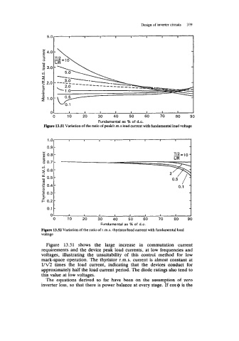
Figure 13.51 shows the large increase in commutation current
requirements and the device peak load currents, at low frequencies and
voltages, illustrating the unsuitability of this control method for low
mark-space operation. The thyristor r.m.s. current is almost constant at
l/d2 times the load current, indicating that the devices conduct for
approximately half the load current period. The diode ratings also tend to
this value at low voltages.
The equations derived so far have been on the assumption of zero
inverter loss, so that there is power balance at every stage. If cos$ is the