
Page 353 - Power Electronics Handbook
P. 353
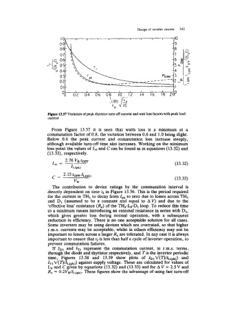
Design of  inverter circuits   343


                                                                               -9


                             0.1 -                                               I


                       Flgure 13.57 Variation of peak thyristor turn-off current and watt loss factors with peak load
                       current

                         From  Figure  13.57  it  is  seen  that  watts  loss  is  a  minimum  at  a
                       commutation factor of  0.8, the variation between 0.6 and 1.0 being slight.
                       Below  0.6  the  peak  current  and  commutation  loss  increase  steeply,
                       although available turn-off time also increases. Working on the minimum
                       loss point the values of Lo and C can be found as in equations (13.32) and
                       (13.33), respectively.

                                                                                 (13.32)


                                                                                 (13.33)
                         The  contribution  to  device  ratings  by  the  commutation  interval  is
                       directly dependent on time r2  in Figure 13.56. This is the period required
                       for the current in TH1 to decay from Zpk  to zero due to losses across TH,
                       and  D1 (assumed to  be  a  constant and  equal to  Av)  and  due to  the
                       'effective loss' resistance (Re) of the THI-L-D1 loop. To reduce this time
                       to a minimum means introducing an external resistance in series with D1,
                       which  gives  greater  loss  during  normal  operation, with  a  subsequent
                       reduction in efficiency. There is no one acceptable solution for all cases.
                       Some inverters may be using devices which are overrated, so  that higher
                       r.m.s. currents may be acceptable, whilst in others efficiency may  not be
                       important so losses across a larger Re are tolerated. In any case it is always
                       important to ensure that rz is less than half a cycle of inverter operation, to
                       prevent commutation failures.
                         If  ZD1 and  ZT1 represent  the  commutation  current,  in  r.m.s. terms,
                       through the diode and thyristor respectively, and Tis the inverter periodic
                       time,  Figures  13.58  and  13.59  show  plots  of  ZDl~(Z")/Zupk~)  and
                                     against
                       &d(7')/lqpk~) supply voltage. These are calculated €or values of
                          and C given by equations (13.32) and (13.33) and for A V = 2.5 V and
                       Re = O.~VB/Z~(~~). figures show the advantage of using fast turn-off
                                        These