
Page 352 - Power Electronics Handbook
P. 352
342 D.C. link frequency changers
Current
thyristor TH,
Current
thyristor TH,
Current diode D,
Voltage D,
0
Voltage D,
Voltage
0
Voltage
Fired
t2
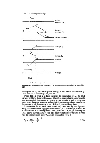
Figure 13.56 Circuit waveforms for Figure 13.55 during the commutation interval of thyristor
TH,
through diode D1 and is dissipated, falling to zero after a further time t2.
Load current is carried by lR, and D1.
When TH2 is fired at a later interval, to commutate TI&, the load
current will have decayed to ZL(-). Therefore commutation requirements
and increased device ratings are not as severe as before, and in the worst
case, when there are no zero dwell periods in the output voltage waveform,
the ratings of all devices are equal. This will be considered here.
If tF denotes the turn-off (reverse voltage) time seen by the thyristor
being commutated and PmM is the watts loss per cornmutation, caused by
the dissipation of the energy stored in Lo, equal to 1/2tO(f,,k)2, then Figure
13.57 shows the variation of turn off, peak current and watts loss factors
with the commutation factor F,, given by equation (13.31).
(13.31)