
Page 281 - Power Electronics Handbook
P. 281
D.C. to d.c. convener circuits 271
resonant paths. For zero loss the voltage would reach an infinite value. To
limit this voltage boost a free-wheeling diode is sometimes connected
across b. This means that when C has discharged to zero volts the energy
stored in is dissipated in the free-wheel path and there is no build-up of
capacitor voltage. The price paid is loss of efficiency.
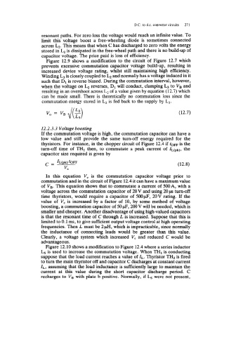
Figure 12.9 shows a modification to the circuit of Figure 12.7 which
prevents excessive commutation capacitor voltage build-up, resulting in
increased device voltage rating, whilst still maintaining high efficiency.
Winding L3 is closely coupled to and normally has a voltage induced in it
such that D1 is reverse biased. During the commutation interval, however,
when the voltage on reverses, D1 will conduct, clamping to VB and
resulting in an overshoot across L, of a value given by equation (1 2.7) which
can be made small. There is theoretically no commutation loss since the
commutation energy stored in L2 is fed back to the supply by L3.
(12.7)
12.2.3.3 Voltage boosting
If the commutation voltage is high, the commutation capacitor can have a
low value and still provide the same turn-off energy required for the
thyristors. For instance, in the chopper circuit of Figure 12.4 if tom is the
turn-off time of THI then, to commutate a peak current of tL(pk), the
capacitor size required is given by
C= IL(pk) fOFF (12.8)
vc
In this equation V, is the commutation capacitor voltage prior to
commutation and in the circuit of Figure 12.4 it can have a maximum value
of VB. This equation shows that to commutate a current of 500A, with a
voltage across the commutation capacitor of 20V and using 20 ps turn-off
time thyristors, would require a capacitor of 500pF, 20V rating. If the
value of V, is increased by a factor of 10, by some method of voltage
boosting, a commutation capacitor of 50 pF, 200 V will be needed, which is
smaller and cheaper. Another disadvantage of using high-valued capacitors
is that the resonant time of C through L is increased. Suppose that this is
limited to 0.1 ms, to give sufficient output voltage control at high operating
frequencies. Then L must be 2 pH, which is impracticable, since normally
the inductance of connecting leads would be greater than this value.
Clearly, a voltage system which increased V, and reduced C would be
advantageous.
Figure 12.10 shows a modification to Figure 12.4 where a series inductor
Ls is used to increase the commutation voltage. When TH, is conducting
suppose that the load current reaches a value of 1,. Thyristor TH2 is fired
to turn the main thyristor off and capacitor C discharges at constant current
Z,, assuming that the load inductance is sufficiently large to maintain the
current at this value during the short capacitor discharge period. C
recharges to Vs with plate b positive. Normally, if were not present,