Page 261 - Rashid, Power Electronics Handbook
P. 261

250                                                                                           J. Espinoza

               where V on  is the rms ac output phase voltage, I o1  is the rms  inverters in the following, although similar results are obtained
               fundamental line current, and f is an arbitrary ®lter-load  for single-phase VSIs.
               angle. Hence, the dc link voltage expression can be further
               simpli®ed to the following:
                                                                    14.5.1 Feedforward Techniques in Voltage
                                                                           Source Inverters
                            I o1          p  I o1
                     v ðtÞ¼ 3  V cosðfÞ¼   3   V cosðfÞ     ð14:61Þ  The dc link bus voltage in VSIs is usually considered a constant
                                                o
                      i
                                on
                             I               I
                             i                i
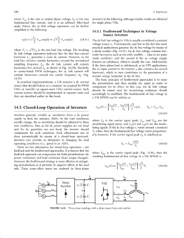
                                                                    voltage source v . Unfortunately, and due to the fact that most
                                                                                 i
                          p                                      practical applications generate the dc bus voltage by means of
               where V ¼   3V   is the rms load line voltage. The resulting
                      o       on                                    a diode recti®er (Fig. 14.35), the dc bus voltage contains low-
               dc link voltage expression indicates that the ®rst line-current
                                                                    order harmonics such as the sixth, twelfth,... (due to six-pulse
               harmonic I  generates a clean dc current. However, as the
                         o1                                         diode recti®ers), and the second if the ac voltage supply
               load line currents contain harmonics around the normalized
                                                                    features an unbalance, which is usually the case. Additionally,
               sampling frequency f , the dc link current will contain  if the three-phase load is unbalanced, as in UPS applications,
                                  sn
               harmonics but around f sn  as shown in Fig. 14.33h. Similarly,  the dc input current in the inverter i also contains the second
                                                                                                  i
               in carrier-based PWM techniques, the dc link current will
                                                                    harmonic, which in turn contributes to the generation of a
               contain harmonics around the carrier frequency m (Fig.  second voltage harmonic in the dc bus.
                                                            f
               14.25).
                                                                      The basic principle of feedforward approaches is to sense
                 In practical implementations, a CSI requires a dc current
                                                                    the perturbation and then modify the input in order to
               source that should behave as a constant (as required by PWM
                                                                    compensate for its effect. In this case, the dc link voltage
               CSIs) or variable (as square-wave CSIs) current source. Such
                                                                    should be sensed and the modulating technique should
               current sources should be implemented as separate units and
                                                                    accordingly be modi®ed. The fundamental ab line voltage in
               they are described earlier in this book.
                                                                    a VSI SPWM can be written as
                                                                                              p
                                                                                               
                                                                               v ðtÞ   v ðtÞ   3
                                                                                        cb1
                                                                                ca1
               14.5 Closed-Loop Operation of Inverters                v ab1 ðtÞ¼  ^ v D  ÿ  ^ v D  2  v ðtÞ;  ^ v > ^ v ; ^ v cb1
                                                                                                          D
                                                                                                              ca1
                                                                                                 i
                                                                                                                 ð14:62Þ
               Inverters generate variable ac waveforms from a dc power
               supply to feed, for instance, ASDs. As the load conditions  where ^ v  is the carrier signal peak, ^ v  and ^ v  are the
               usually change, the ac waveforms should be adjusted to these  D                       ca1     cb1
                                                                                              ca
                                                                                                      cb
               new conditions. Also, as the dc power supplies are not ideal  modulating signal peaks, and v ðtÞ and v ðtÞ are the modu-
                                                                    lating signals. If the dc bus voltage v varies around a nominal
                                                                                                 i
               and the dc quantities are not ®xed, the inverter should  V value, then the fundamental line voltage varies proportion-
               compensate for such variations. Such adjustments can be  i
                                                                    ally; however, if the carrier signal peak ^ v is rede®ned as
               done automatically by means of a closed-loop approach.                                D
               Inverters also provide an alternative to changing the load
                                                                                               v ðtÞ
                                                                                                i
               operating conditions (i.e., speed in an ASD).                            ^ v ¼ ^ v Dm             ð14:63Þ
                                                                                        D
                 There are two alternatives for closed-loop operation Ð the                     V i
               feedback and the feedforward approaches. It is known that the
                                                                    where ^ v  is the carrier signal peak (Fig. 14.36), then the
               feedback approach can compensate for both perturbations (dc  Dm
                                                                    resulting fundamental ab line voltage in a VSI SPWM is
               power variations) and load variations (load torque changes).
               However, the feedforward strategy is more effective in mitigat-                      p 
               ing perturbations as it prevents its negative effects at the load  v ab1 ðtÞ¼  v ðtÞ  ÿ  v ðtÞ  3  V i  ð14:64Þ
                                                                                      ca1
                                                                                              cb1
               side. These cause-effect issues are analyzed in three-phase             ^ v Dm  ^ v Dm  2
                                        FIGURE 14.35  Three-phase topology with a diode-based front-end recti®er.
   256   257   258   259   260   261   262   263   264   265   266