
Page 276 - Rashid, Power Electronics Handbook
P. 276
14 Inverters 265
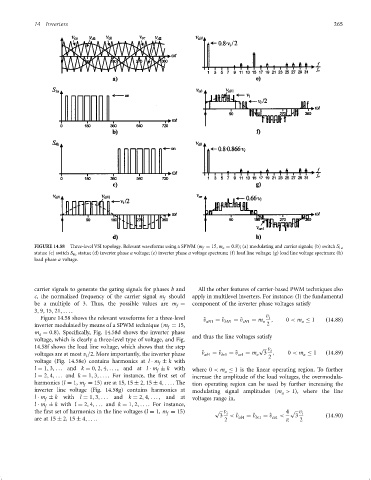
FIGURE 14.58 Three-level VSI topology. Relevant waveforms using a SPWM (m f ¼ 15, m a ¼ 0:8); (a) modulating and carrier signals; (b) switch S 1a
status; (c) switch S 4b status; (d) inverter phase a voltage; (e) inverter phase a voltage spectrum; (f) load line voltage; (g) load line voltage spectrum; (h)
load phase a voltage.
carrier signals to generate the gating signals for phases b and All the other features of carrier-based PWM techniques also
c, the normalized frequency of the carrier signal m should apply in multilevel inverters. For instance: (I) the fundamental
f
be a multiple of 3. Thus, the possible values are m ¼ component of the inverter phase voltages satisfy
f
3; 9; 15; 21; ... .
Figure 14.58 shows the relevant waveforms for a three-level ^ v aN1 ¼ ^ v bN1 ¼ ^ v cN1 ¼ m a v i ; 0 < m 1 ð14:88Þ
a
inverter modulated by means of a SPWM technique (m ¼ 15, 2
f
m ¼ 0:8). Speci®cally, Fig. 14.58d shows the inverter phase
a
voltage, which is clearly a three-level type of voltage, and Fig. and thus the line voltages satisfy
14.58f shows the load line voltage, which shows that the step p v i
voltages are at most v =2. More importantly, the inverter phase ^ v ab1 ¼ ^ v bc1 ¼ ^ v ca1 ¼ m a 3 ; 0 < m 1 ð14:89Þ
a
i 2
voltage (Fig. 14.58e) contains harmonics at l m k with
f
l ¼ 1; 3; ... and k ¼ 0; 2; 4; .. . , and at l m k with
f where 0 < m 1 is the linear operating region. To further
a
l ¼ 2; 4; ... and k ¼ 1; 3; ... . For instance, the ®rst set of increase the amplitude of the load voltages, the overmodula-
harmonics (l ¼ 1, m ¼ 15) are at 15, 15 2; 15 4; ... . The
f tion operating region can be used by further increasing the
inverter line voltage (Fig. 14.58g) contains harmonics at modulating signal amplitudes (m > 1), where the line
a
l m k with l ¼ 1; 3; ... and k ¼ 2; 4; ... , and at voltages range in,
f
l m k with l ¼ 2; 4; ... and k ¼ 1; 2; ... . For instance,
f
the ®rst set of harmonics in the line voltages ðl ¼ 1, m ¼ 15) p v i 4 p v i
f
are at 15 2, 15 4; ... . 3 2 < ^ v ab1 ¼ ^ v bc1 ¼ ^ v ca1 < p 3 2 ð14:90Þ