
Page 275 - Rashid, Power Electronics Handbook
P. 275
264 J. Espinoza
tance) smoothes out the edges of the current, which also TABLE 14.7 Valid switch states for a three-level VSI, phase a
contributes to the reactive power required by the cells. This
last effect is not shown in Fig. 14.56a,b and c. S 1a S 1b S 4a S 4b v o Components Conducting
1 1 0 0 v i =2 S 1a , S 1b if i oa > 0
if i oa < 0
D 1a , D 1b
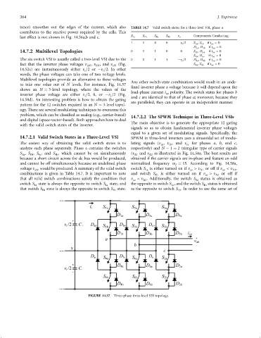
14.7.2 Multilevel Topologies 0 1 1 0 0 S 1b , D aþ if i oa > 0
if i oa < 0
S 4a , D aÿ
The six-switch VSI is usually called a two-level VSI due to the 0 0 1 1 ÿv i =2 D 4a , D 4b if i oa > 0
fact that the inverter phase voltages v , v , and v cN (Fig. S 4a , S 4b if i oa < 0
aN
bN
14.52a) are instantaneously either v =2or ÿv =2. In other
i
i
words, the phase voltages can take one of two voltage levels.
Multilevel topologies provide an alternative to these voltages
Any other switch-state combination would result in an unde-
to take one value out of N levels. For instance, Fig. 14.57
®ned inverter phase a voltage because it will depend upon the
shows an N ¼ 3-level topology, where the values of the load-phase current i polarity. The switch states for phases b
inverter phase voltage are either v =2, 0, or ÿv =2 (Fig. oa
i i and c are identical to that of phase a; moreover, because they
14.58d). An interesting problem is how to obtain the gating
are paralleled, they can operate in an independent manner.
pattern for the 12 switches required in an N ¼ 3-level topol-
ogy. There are several modulating techniques to overcome this
problem, which can be classi®ed as analog (e.g., carrier-based) 14.7.2.2 The SPWM Technique in Three-Level VSIs
and digital (space-vector-based). Both approaches have to deal
The main objective is to generate the appropriate 12 gating
with the valid switch states of the inverter.
signals so as to obtain fundamental inverter phase voltages
equal to a given set of modulating signals. Speci®cally, the
14.7.2.1 Valid Switch States in a Three-Level VSI SPWM in three-level inverters uses a sinusoidal set of modu-
The easiest way of obtaining the valid switch states is to lating signals (v , v , and v cc for phases a, b, and c,
cb
ca
analyze each phase separately. Phase a contains the switches respectively) and N ÿ 1 ¼ 2 triangular type of carrier signals
S , S , S , and S , which cannot be on simultaneously (v D1 and v D2 as illustrated in Fig. 14.58a. The best results are
4a
1b
1a
4b
because a short circuit across the dc bus would be produced, obtained if the carrier signals are in-phase and feature an odd
and cannot be off simultaneously because an unde®ned phase normalized frequency m ¼ 15. According to Fig. 14.58a,
f
voltage v aN would be produced. A summary of the valid switch switch S 1a is either turned on if v > v D1 or off if v < v ,
ca
D1
ca
combinations is given in Table 14.7. It is important to note and switch S 1b is either turned on if v > v D2 or off if
ca
that all valid switch combinations satisfy the condition that v < v . Additionally, the switch S 4a status is obtained as
D2
ca
switch S 1a state is always the opposite to switch S 4a state, and the opposite to switch S , and the switch S status is obtained
1a
4b
that switch S state is always the opposite to switch S state. as the opposite to switch S . In order to use the same set of
1b 4b 1b
FIGURE 14.57 Three-phase three-level VSI topology.