
Page 277 - Rashid, Power Electronics Handbook
P. 277
266 J. Espinoza
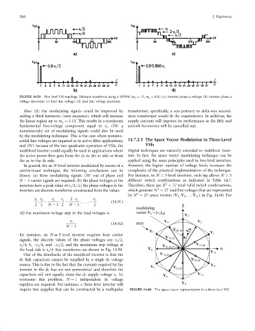
FIGURE 14.59 Five-level VSI topology. Relevant waveforms using a SPWM (m f ¼ 15, m a ¼ 0:8): (a) inverter phase a voltage; (b) inverter phase a
voltage spectrum; (c) load line voltage; (d) load line voltage spectrum.
Also: (II) the modulating signals could be improved by transformer; speci®cally, a wye primary to delta-wye second-
adding a third harmonic (zero sequence), which will increase aries transformer would ®t the requirements. In addition, the
the linear region up to m ¼ 1:15. This results in a maximum supply currents will improve its performance as the ®fth and
a
fundamental line-voltage component equal to v . (III) a seventh harmonics will be cancelled out.
i
nonsinusoidal set of modulating signals could also be used
by the modulating technique. This is the case where nonsinu-
soidal line voltages are required as in active ®lter applications; 14.7.2.3 The Space Vector Modulation in Three-Level
and (IV) because of the two quadrants operation of VSIs, the VSIs
multilevel inverter could equally be used in applications where Digital techniques are naturally extended to multilevel inver-
the active power ¯ow goes from the dc to the ac side or from ters. In fact, the space vector modulating technique can be
the ac to the dc side. applied using the same principles used in two-level inverters.
In general, for an N-level inverter modulated by means of a However, the higher number of voltage levels increases the
carrier-based technique, the following conclusions can be complexity of the practical implementation of the technique.
drawn: (a) three modulating signals 120 out of phase and For instance, in N ¼ 3-level inverters, each leg allows N ¼ 3
N ÿ 1 carrier signals are required; (b) the phase voltages in the different switch combinations as indicated in Table 14.7.
3
inverters have a peak value of v =2; (c) the phase voltages in the Therefore, there are N ¼ 27 total valid switch combinations,
i
3
inverters are discrete waveforms constructed from the values which generate N ¼ 27 load line voltages that are represented
3
by N ¼ 27 space vectors (V ; V ; ... V ) in Fig. 14.60. For
2
1
27
v v i ÿ v i ; v i ÿ 2 v i ; ... ; ÿ v i ð14:91Þ
i
;
2 2 N ÿ 1 2 N ÿ 1 2
(d) the maximum voltage step in the load voltages is
v i
ð14:92Þ
N ÿ 1
for instance, an N ¼ 5-level inverter requires four carrier
signals, the discrete values of the phase voltages are: v =2,
i
v =4, 0, ÿv =4, and ÿv =2, and the maximum step voltage at
i
i
i
the load side is v =4. Key waveforms are shown in Fig. 14.59.
i
One of the drawbacks of the multilevel inverter is that the
dc link capacitors cannot be supplied by a single dc voltage
source. This is due to the fact that the currents required by the
inverter in the dc bus are not symmetrical and therefore the
capacitors will not equally share the dc supply voltage v .To
i
overcome this problem, N ÿ 1 independent dc voltage
supplies are required. For instance, a three-level inverter will
require two supplies that can be constructed by a multipulse FIGURE 14.60 The space vector representation in a three-level VSI.