
Page 291 - Semiconductor Manufacturing Handbook
P. 291
Geng(SMH)_CH19.qxd 04/04/2005 20:00 Page 19.18
INSPECTION, MEASUREMENT, AND TEST
19.18 FINAL MANUFACTURING
Shmoo plots depict two or three of these sweep parameters tested across a range for each, and the
pass/fail results plotted in an XY(Z) plot. This not only shows the limits of the parameters, but also
indicates how the parameters interact with one another.
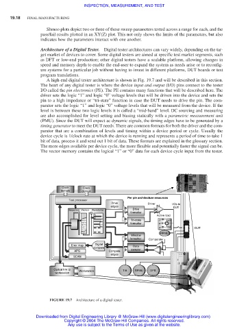
Architecture of a Digital Tester. Digital tester architectures can vary widely, depending on the tar-
get market of devices to cover. Some digital testers are aimed at specific test market segments, such
as DFT or low-end production; other digital testers have a scalable platform, allowing changes in
speed and memory depth to enable the end-user to expand the system as needs arise or to reconfig-
ure systems for a particular job without having to invest in different platforms, DUT boards or test
program translations.
A high-end digital tester architecture is shown in Fig. 19.7 and will be described in this section.
The heart of any digital tester is where the device input and output (I/O) pins connect to the tester
I/O called the pin electronics (PE). The PE contains many functions that will be described here. The
driver sets the logic “1” and logic “0” voltage levels that will be driven into the device and sets the
pin to a high impedance or “tri-state” function in case the DUT needs to drive the pin. The com-
parator sets the logic “1” and logic “0” voltage levels that will be measured from the device. If the
level is between these two logic levels it is called a “mid-band” level. DC sourcing and measuring
are also accomplished for level setting and biasing statically with a parametric measurement unit
(PMU). Since the DUT will expect ac dynamic signals, the timing edges have to be generated by a
timing generator to meet the DUT needs. There are common formats for both the driver and the com-
parator that are a combination of levels and timing within a device period or cycle. Usually the
device cycle is 1/clock rate at which the device is running and represents a period of time to take 1
bit of data, process it and send out 1 bit of data. These formats are explained in the glossary section.
The more edges available per device cycle, the more flexible and potentially faster the signal can be.
The vector memory contains the logical “1” or “0” data for each device cycle input from the tester.
Clock Clock
domain domain
Per pin architecture resources
Test processor
Drive Driver I/Os to
edges DUT
Drive
Sequencer Vectors Waveforms
formatter
Active load
0
0 000
0 000 Tri-state Ioh
0 0 10 formatter
000 1 r
0011 Iol DUT
0110
0010
PPMU
Window
formatter Comparator
Error map Digital Data
compare
APG Compare sampler
edges
SCAN
Optical link to Workstation TIA SPMU DPS
workstation
FIGURE 19.7 Architecture of a digital tester.
Downloaded from Digital Engineering Library @ McGraw-Hill (www.digitalengineeringlibrary.com)
Copyright © 2004 The McGraw-Hill Companies. All rights reserved.
Any use is subject to the Terms of Use as given at the website.