
Page 120 - Wire Bonding in Microelectronics
P. 120
W ir e Bond Testing 99
thin films. Therefore, ball-shear tests made on thick-film circuits
may present problems in vertical positioning of the tool. It is, there-
fore, possible that the tool will drag across the thick film during the
shear process. This will result in a high-apparent value for the ball-
shear force and may explain why some reported values of ball-shear
force from thick-film tests are higher than the shear force expected
from thin film Au [4-21].
Even if the vertical positioning of the shear tool is correct, shear
tests made on bonds welded to thick films, as well as to thin films,
can yield much lower shear values than expected if the metalliza-
tion adheres poorly to the substrate [4-11, 4-14]. An example of
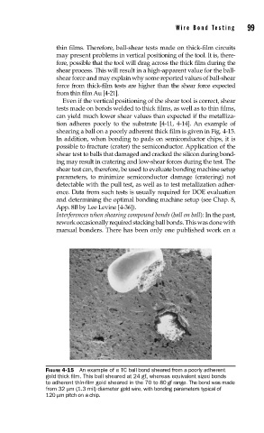
shearing a ball on a poorly adherent thick film is given in Fig. 4-15.
In addition, when bonding to pads on semiconductor chips, it is
possible to fracture (crater) the semiconductor. Application of the
shear test to balls that damaged and cracked the silicon during bond-
ing may result in cratering and low-shear forces during the test. The
shear test can, therefore, be used to evaluate bonding machine setup
parameters, to minimize semiconductor damage (cratering) not
detectable with the pull test, as well as to test metallization adher-
ence. Data from such tests is usually required for DOE evaluation
and determining the optimal bonding machine setup (see Chap. 8,
App. 8B by Lee Levine [4-36]).
Interferences when shearing compound bonds (ball on ball): In the past,
rework occasionally required stacking ball bonds. This was done with
manual bonders. There has been only one published work on a
FIGURE 4-15 An example of a TC ball bond sheared from a poorly adherent
gold thick fi lm. This ball sheared at 24 gf, whereas equivalent sized bonds
to adherent thin-fi lm gold sheared in the 70 to 80 gf range. The bond was made
from 32 µm (1.3 mil) diameter gold wire, with bonding parameters typical of
120 µm pitch on a chip.