
Page 165 - Wire Bonding in Microelectronics
P. 165
142 Cha pte r F i v e
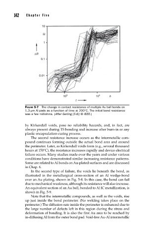
10
Ω
1
∆R
0.1
0.01
10 3 10 4 h
t
FIGURE 5-7 The change in contact resistance of multiple Au ball bonds on
1.3 µm Al pads as a function of time at 200°C. The initial bond resistance
was a few milliohms. (After Gerling [5-8]; © IEEE.)
by Kirkendall voids, pose no reliability hazards, and, in fact, are
always present during TS bonding and increase after burn-in or any
plastic encapsulation-curing process.
The second resistance increase occurs as the intermetallic com-
pound continues forming outside the actual bond area and around
the perimeter. Later, as Kirkendall voids form (e.g., several thousand
hours at 150°C), the resistance increases rapidly and device electrical
failure occurs. Many studies made over the years and under various
conditions have demonstrated similar increasing resistance patterns.
Some are related to Al bonds on Au-plated surfaces and are discussed
in Chap. 6.
In the second type of failure, the voids lie beneath the bond, as
illustrated in the metallurgical cross-section of an Al wedge-bond
over an Au plating, shown in Fig. 5-8. In this case, the bond can fail
due to mechanical weakness, although its resistance will also increase.
An equivalent section of an Au ball, bonded to Al IC metallization, is
shown in Fig. 5-9.
Note that the intermetallic compounds, as well as the voids, rise
up just inside the bond perimeter. (No welding takes place on the
perimeter.) The diffusion rate inside the perimeter is enhanced due to
the large number of defects left in this region during the stress and
deformation of bonding. It is also the first Au area to be reached by
in-diffusing Al from the outer bond pad. Void-free Au-Al intermetallic