
Page 119 -
P. 119
92 CHAPTER 3 / A TOP-LEVEL VIEW OF COMPUTER FUNCTION
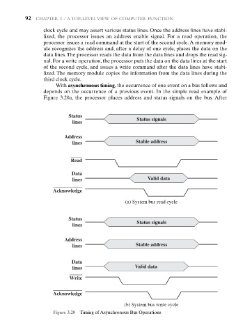
clock cycle and may assert various status lines. Once the address lines have stabi-
lized, the processor issues an address enable signal. For a read operation, the
processor issues a read command at the start of the second cycle. A memory mod-
ule recognizes the address and, after a delay of one cycle, places the data on the
data lines.The processor reads the data from the data lines and drops the read sig-
nal. For a write operation, the processor puts the data on the data lines at the start
of the second cycle, and issues a write command after the data lines have stabi-
lized. The memory module copies the information from the data lines during the
third clock cycle.
With asynchronous timing, the occurrence of one event on a bus follows and
depends on the occurrence of a previous event. In the simple read example of
Figure 3.20a, the processor places address and status signals on the bus. After
Status
Status signals
lines
Address
lines Stable address
Read
Data
lines Valid data
Acknowledge
(a) System bus read cycle
Status
Status signals
lines
Address
lines Stable address
Data
lines Valid data
Write
Acknowledge
(b) System bus write cycle
Figure 3.20 Timing of Asynchronous Bus Operations