
Page 124 -
P. 124
3.5 / PCI 97
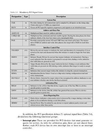
Table 3.3 Mandatory PCI Signal Lines
Designation Type Description
System Pins
CLK in Provides timing for all transactions and is sampled by all inputs on the rising edge.
Clock rates up to 33 MHz are supported.
RST# in Forces all PCI-specific registers, sequencers, and signals to an initialized state.
Address and Data Pins
AD[31::0] t/s Multiplexed lines used for address and data
C/BE[3::0]# t/s Multiplexed bus command and byte enable signals. During the data phase, the lines
indicate which of the four byte lanes carry meaningful data.
PAR t/s Provides even parity across AD and C/BE lines one clock cycle later.The master
drives PAR for address and write data phases; the target drive PAR for read data
phases.
Interface Control Pins
FRAME# s/t/s Driven by current master to indicate the start and duration of a transaction. It is as-
serted at the start and deasserted when the initiator is ready to begin the final data
phase.
IRDY# s/t/s Initiator Ready. Driven by current bus master (initiator of transaction). During a
read, indicates that the master is prepared to accept data; during a write, indicates
that valid data are present on AD.
TRDY# s/t/s Target Ready. Driven by the target (selected device). During a read, indicates that
valid data are present on AD; during a write, indicates that target is ready to accept
data.
STOP# s/t/s Indicates that current target wishes the initiator to stop the current transaction.
IDSEL in Initialization Device Select. Used as a chip select during configuration read and
write transactions.
DEVSEL# in Device Select.Asserted by target when it has recognized its address. Indicates to cur-
rent initiator whether any device has been selected.
Arbitration Pins
REQ# t/s Indicates to the arbiter that this device requires use of the bus.This is a device-
specific point-to-point line.
GNT# t/s Indicates to the device that the arbiter has granted bus access.This is a device-
specific point-to-point line.
Error Reporting Pins
PERR# s/t/s Parity Error. Indicates a data parity error is detected by a target during a write data
phase or by an initiator during a read data phase.
SERR# o/d System Error. May be pulsed by any device to report address parity errors and
critical errors other than parity.
In addition, the PCI specification defines 51 optional signal lines (Table 3.4),
divided into the following functional groups:
• Interrupt pins: These are provided for PCI devices that must generate re-
quests for service. As with the arbitration pins, these are not shared lines.
Rather, each PCI device has its own interrupt line or lines to an interrupt
controller.