
Page 125 -
P. 125
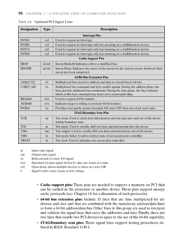
98  CHAPTER 3 / A TOP-LEVEL VIEW OF COMPUTER FUNCTION

           Table 3.4 Optional PCI Signal Lines

            Designation  Type                          Description
                                              Interrupt Pins
            INTA#        o/d   Used to request an interrupt.
            INTB#        o/d   Used to request an interrupt; only has meaning on a multifunction device.
            INTC#        o/d   Used to request an interrupt; only has meaning on a multifunction device.
            INTD#        o/d   Used to request an interrupt; only has meaning on a multifunction device.
                                            Cache Support Pins
            SBO#        in/out  Snoop Backoff. Indicates a hit to a modified line.
            SDONE       in/out  Snoop Done. Indicates the status of the snoop for the current access.Asserted when
                               snoop has been completed.
                                         64-Bit Bus Extension Pins
            AD[63::32]    t/s  Multiplexed lines used for address and data to extend bus to 64 bits.
            C/BE[7::4]#   t/s  Multiplexed bus command and byte enable signals. During the address phase, the
                               lines provide additional bus commands. During the data phase, the lines indicate
                               which of the four extended byte lanes carry meaningful data.
            REQ64#       s/t/s  Used to request 64-bit transfer.
            ACK64#       s/t/s  Indicates target is willing to perform 64-bit transfer.
            PAR64         t/s  Provides even parity across extended AD and C/BE lines one clock cycle later.
                                         JTAG/Boundary Scan Pins
            TCK           in   Test clock. Used to clock state information and test data into and out of the device
                               during boundary scan.
            TDI           in   Test input. Used to serially shift test data and instructions into the device.
            TDO          out   Test output. Used to serially shift test data and instructions out of the device.
            TMS           in   Test mode Select. Used to control state of test access port controller.
            TRST#         in   Test reset. Used to initialize test access port controller.

            in    Input-only signal
            out   Output-only signal
            t/s   Bidirectional, tri-state, I/O signal
            s/t/s  Sustained tri-state signal driven by only one owner at a time
            o/d   Open drain: allows multiple devices to share as a wire-OR
            #     Signal’s active state occurs at low voltage


                     • Cache support pins: These pins are needed to support a memory on PCI that
                       can be cached in the processor or another device. These pins support snoopy
                       cache protocols (see Chapter 18 for a discussion of such protocols).
                     • 64-bit bus extension pins: Include 32 lines that are time multiplexed for ad-
                       dresses and data and that are combined with the mandatory address/data lines
                       to form a 64-bit address/data bus. Other lines in this group are used to interpret
                       and validate the signal lines that carry the addresses and data. Finally, there are
                       two lines that enable two PCI devices to agree to the use of the 64-bit capability.
                     • JTAG/boundary scan pins: These signal lines support testing procedures de-
                       fined in IEEE Standard 1149.1.