
Page 453 - DSP Integrated Circuits
P. 453
438 Chapter 10 Digital Systems
Figure 10.1 Hierarchical decomposition of a digital system
10.2 COMBINATIONAL NETWORKS
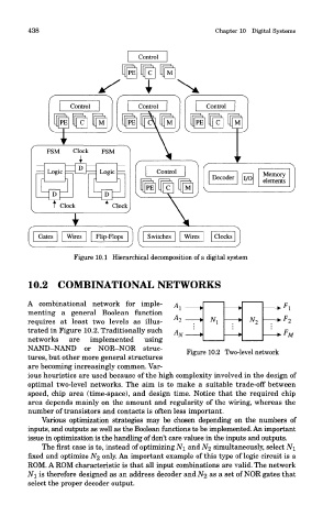
A combinational network for imple-
menting a general Boolean function
requires at least two levels as illus-
trated in Figure 10.2. Traditionally such
networks are implemented using
NAND-NAND or NOR-NOR struc-
Figure 10.2 Two-level network
tures, but other more general structures
are becoming increasingly common. Var-
ious heuristics are used because of the high complexity involved in the design of
optimal two-level networks. The aim is to make a suitable trade-off between
speed, chip area (time-space), and design time. Notice that the required chip
area depends mainly on the amount and regularity of the wiring, whereas the
number of transistors and contacts is often less important.
Various optimization strategies may be chosen depending on the numbers of
inputs, and outputs as well as the Boolean functions to be implemented. An important
issue in optimization is the handling of don't care values in the inputs and outputs.
The first case is to, instead of optimizing NI and A^2 simultaneously, select NI
fixed and optimize A/2 only. An important example of this type of logic circuit is a
ROM. A ROM characteristic is that all input combinations are valid. The network
NI is therefore designed as an address decoder and N% as a set of NOR gates that
select the proper decoder output.