
Page 458 - DSP Integrated Circuits
P. 458
10.4 Storage Elements 443
latch (with J = S and K = R) except that the response to J = K = 1 is that the latch
changes state. This is expressed as
The next state of a D latch is the same as the current input. A JK flip-flop can
be changed into a D flip-flop by letting D = J = K.
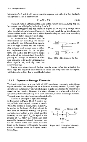
The edge-triggered flip-flop shown in Figure 10.12 may only change state
when the clock signal changes. Changes in the input signal during the clock cycle
have no effect on the stored state, which depends solely on conditions prevailing
immediately before the active clock edge.
A master—slave flip-flop can be
implemented by cascading two latches
controlled by two different clock signals.
Both the type of latch and the relation-
ship between clock signals vary in differ-
ent implementations. In its simplest
form, two latches are driven by a single
clock signal, (£3 being derived from <&i by
passing it through an inverter. A com- Figure 10.12 Edge-triggered flip-flop.
mon variation is to use two independent
clock signals, <£>i and d>2, that are
nonoverlapping.
Inputs to an edge-triggered flip-flop must be stable before the arrival of the
clock edge. The required time interval is called the setup time for the inputs,
which includes a delay due to possible clock skew.
10.4.2 Dynamic Storage Elements
The input capacitance to a gate built of MOS transistors represents a significant
capacitance that can be exploited as a dynamic memory element. Dynamic logic
circuits rely on temporary storage of charges in gate capacitances to simplify and
speed up the circuits. However, the state (charged or uncharged node) of a
dynamic node is retained only for a short time (ms), because of leakage currents.
The node must therefore be recharged periodically.
The basic principle of dynamic storage
is illustrated in Figure 10.13. A control sig-
nal, called a clock signal, controls a switch.
When the switch is closed, input signal Vj n
is applied to the input of a logic circuit, in
this case an inverter. During this phase,
neglecting any delays in the switch and the
inverter, output signal V out is equal to the
inverse of Vi n. After the switch has been
opened by the control signal, the output sig-
nal will remain at the same value, since the
input to the inverter will remain the same Figure 10.13 Principle of a dynamic
due to the charge stored in the gate capaci- storage element
tance, C gate.