
Page 456 - DSP Integrated Circuits
P. 456
10.4 Storage Elements 441
must be valid before and during the positive clock edge to ensure proper operation.
A small delay between input and output is incurred.
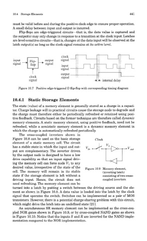
Flip-flops are edge-triggered circuits—that is, the data value is captured and
the output(s) may only change in response to a transition at the clock input. Latches
are level-sensitive circuits—that is, changes at the data input will be observed at the
latch output(s) as long as the clock signal remains at its active level.
Figure 10.7 Positive edge-triggered D flip-flop with corresponding timing diagram
10.4.1 Static Storage Elements
The state (value) of a memory element is generally stored as a charge in a capaci-
tor. Charge leakage will in practical circuits cause the storage node to degrade and
the charge must therefore either be periodically refreshed or retained using posi-
tive feedback. Circuits based on the former technique are therefore called dynamic
memory elements. A static memory element, using positive feedback, need not be
refreshed, while a semistatic memory element is a dynamic memory element in
which the charge is automatically refreshed periodically.
The cross-coupled inverters shown in
Figure 10.8 can be used as the basic storage
element of a static memory cell. The circuit
has a stable state in which the input and out-
put are complementary. The inverter driven
by the output node is designed to have a low
drive capability so that an input signal driv-
ing the memory cell can force node V\ to any
desired value, irrespective of the state of the Figure 10.8 Memory element,
cell. The memory will remain in its stable (inverting latch)
state if the storage element is left without a consisting of two cross-
driving input. Hence, the circuit does not coupled inverters
need refreshing. The memory element can be
turned into a latch by putting a switch between the driving source and the ele-
ment as shown in Figure 10.8. A data value is loaded into the latch by the clock
signal that operates the switch. Switches can be implemented as a pair of MOS
transistors. However, there is a potential charge-sharing problem with this circuit,
which might drive the latch into an undefined state [21].
An asynchronous SR memory element can be implemented as the cross-cou-
pled NOR gates shown in Figure 10.9, or by cross-coupled NAND gates as shown
in Figure 10.10. Notice that the inputs S and R are inverted for the NAND imple-
mentation compared to the NOR implementation.