
Page 457 - DSP Integrated Circuits
P. 457
442 Chapter 10 Digital Systems
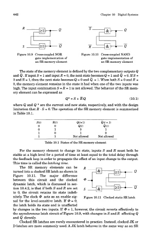
Figure 10.9 Cross-coupled NOR Figure 10.10 Cross-coupled NAND
gate implementation of gate implementation of
an SR memory element an SR memory element
The state of the memory element is defined by the two complementary outputs Q
and Q . If input S = 1 and input R = 0, the next state becomes Q = 1 and Q = 0. If S =
0 and R = l, then the next state becomes Q = 0 and Q = 1. When both S = 0 and R =
0, the memory element remains in the state it had when one of the two inputs was
high. The input combination S = R = 1 is not allowed. The behavior of the SR mem-
ory element can be expressed as
+
where Q and Q are the current and new state, respectively, and with the design
limitation that R • S - 0. The operation of the SR memory element is summarized
in Table 10.1.
S(t) R(t) Q(M-l) Q(t_ + t)
0 0 Q(t) Q(t)
0 1 0 1
1 0 1 0
1 1 Not allowed Not allowed
Table 10.1 States of the SR memory element
For the memory element to change its state, inputs S and R must both be
stable at a high level for a period of time at least equal to the total delay through
the feedback loop in order to propagate the effect of an input change to the output.
This time is called the latching time.
The SR memory elements can be
turned into a clocked SR latch as shown in
Figure 10.11. The major difference
between this circuit and the clocked
dynamic latch, which is discussed in sec-
tion 10.4.2, is that if both S and R are set
to 0, the circuit retains its state indefi-
nitely. The clock 0 acts as an enable sig- Figure 10.11 Clocked static SR latch
nal for the level-sensitive latch. If 0 = 0,
the latch holds its state and is unaffected
by changes in the two inputs. If 0 = 1, however, the circuit reverts effectively to
the asynchronous latch circuit of Figure 10.9, with changes in S and R affecting Q
and Q directly.
Clocked SR latches are rarely encountered in practice. Instead, clocked JK or
D latches are more commonly used. A JK latch behaves in the same way as an SR