
Page 462 - DSP Integrated Circuits
P. 462
10.5 Clocking of Synchronous Systems 447
Another disadvantage is the voltage variations that may occur at the output
of a block due to evaluation time in the block. This results in peaks in the output
voltage of a p-block, when it is low for two consecutive clock periods, on a negative
clock transition. For an n-block the opposite situation occurs with voltage drops on
positive clock transitions when the output is high. Neither of these cases cause
problems in single-phase logic, but connections to other kinds of logic have to be
made with caution.
An advantage is that
only one clock wire needs to
be distributed over the logic
circuitry, resulting in fewer
clock drivers and no clock
skew. However, the require-
ment on sharp clock edges is
strict.
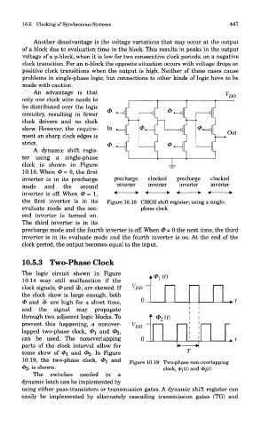
A dynamic shift regis-
ter using a single-phase
clock is shown in Figure
10.18. When 0 = 0, the first
inverter is in its precharge
mode and the second
inverter is off. When 0 = 1,
the first inverter is in its Figure 10.18 CMOS shift register; using a single-
evaluate mode and the sec- phase clock
ond inverter is turned on.
The third inverter is in its
precharge mode and the fourth inverter is off. When 0=0 the next time, the third
inverter is in its evaluate mode and the fourth inverter is on. At the end of the
clock period, the output becomes equal to the input.
10.5.3 Two-Phase Clock
The logic circuit shown in Figure
10.14 may still malfunction if the
clock signals, 0 and &, are skewed. If
the clock skew is large enough, both
0 and €> are high for a short time,
and the signal may propagate
through two adjacent logic blocks. To
prevent this happening, a nonover-
lapped two-phase clock, 4>i and 02,
can be used. The nonoverlapping
parts of the clock interval allow for
1
some skew of 0\ and 02- I* Figure
10.19, the two-phase clock, 0± and Figure 10.19 Two-phase non-overlapping
3>2, is shown. clock, <PI(£) and &z(t)
The switches needed in a
dynamic latch can be implemented by
using either pass-transistors or transmission gates. A dynamic shift register can
easily be implemented by alternately cascading transmission gates (TG) and