
Page 461 - DSP Integrated Circuits
P. 461
446 Chapter 10 Digital Systems
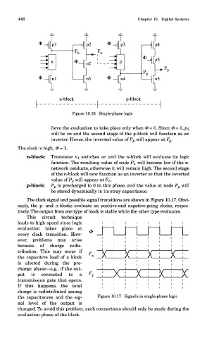
Figure 10.16 Single-phase logic
force the evaluation to take place only when 3> = 0. Since 0 = 0,ps
will be on and the second stage of the p-block will function as an
inverter. Hence, the inverted value of P p will appear at F p.
The clock is high, 0=1.
n-block: Transistor n\ switches on and the n-block will evaluate its logic
function. The resulting value of node P n will become low if the n-
network conducts, otherwise it will remain high. The second stage
of the n-block will now function as an inverter so that the inverted
value of P n will appear at F n.
p-block: Pp is precharged to 0 in this phase, and the value at node F p will
be stored dynamically in its stray capacitance.
The clock signal and possible signal transitions are shown in Figure 10.17. Obvi-
ously, the p- and n-blocks evaluate on positive-and negative-going clocks, respec-
tively. The output from one type of block is stable while the other type evaluates.
This circuit technique
leads to high speed since logic
evaluation takes place at
every clock transition. How-
ever, problems may arise
because of charge redis-
tribution. This may occur if
the capacitive load of a block
is altered during the pre-
charge phase—e.g., if the out-
put is connected to a
transmission gate that opens.
If this happens, the total
charge is redistributed among
the capacitances and the sig- Figure 10.17 Signals in single-phase logic
nal level of the output is
changed. To avoid this problem, such connections should only be made during the
evaluation phase of the block.