
Page 460 - DSP Integrated Circuits
P. 460
10.5 Clocking of Synchronous Systems 445
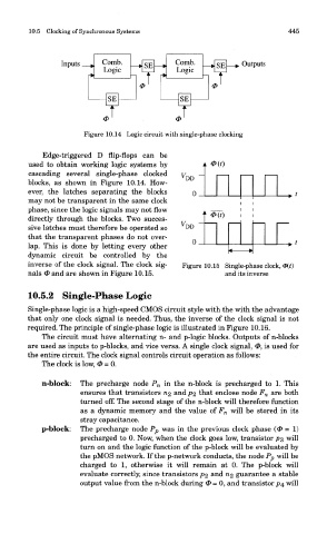
Figure 10.14 Logic circuit with single-phase clocking
Edge-triggered D flip-flops can be
used to obtain working logic systems by
cascading several single-phase clocked
blocks, as shown in Figure 10.14. How-
ever, the latches separating the blocks
may not be transparent in the same clock
phase, since the logic signals may not flow
directly through the blocks. Two succes-
sive latches must therefore be operated so
that the transparent phases do not over-
lap. This is done by letting every other
dynamic circuit be controlled by the
inverse of the clock signal. The clock sig- Figure 10.15 Single-phase clock, <t>(t)
nals <P and are shown in Figure 10.15. and its inverse
10.5.2 Single-Phase Logic
Single-phase logic is a high-speed CMOS circuit style with the with the advantage
that only one clock signal is needed. Thus, the inverse of the clock signal is not
required. The principle of single-phase logic is illustrated in Figure 10.16.
The circuit must have alternating n- and p-logic blocks. Outputs of n-blocks
are used as inputs to p-blocks, and vice versa. A single clock signal, 0, is used for
the entire circuit. The clock signal controls circuit operation as follows:
The clock is low, <P = 0.
n-block: The precharge node P n in the n-block is precharged to 1. This
ensures that transistors n% and P2 that enclose node F n are both
turned off. The second stage of the n-block will therefore function
as a dynamic memory and the value of F n will be stored in its
stray capacitance.
p-block: The precharge node P p was in the previous clock phase (0=1)
precharged to 0. Now, when the clock goes low, transistor pa will
turn on and the logic function of the p-block will be evaluated by
the pMOS network. If the p-network conducts, the node P p will be
charged to 1, otherwise it will remain at 0. The p-block will
evaluate correctly, since transistors p2 and n<z guarantee a stable
output value from the n-block during 3> = 0, and transistor p4 will