
Page 463 - DSP Integrated Circuits
P. 463
448 Chapter 10 Digital Systems
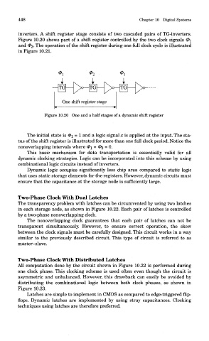
inverters. A shift register stage consists of two cascaded pairs of TG-inverters.
Figure 10.20 shows part of a shift register controlled by the two clock signals <2>i
and 02- The operation of the shift register during one full clock cycle is illustrated
in Figure 10.21.
Figure 10.20 One and a half stages of a dynamic shift register
The initial state is 0i = 1 and a logic signal x is applied at the input. The sta-
tus of the shift register is illustrated for more than one full clock period. Notice the
nonoverlapping intervals where <2>i = (^2 = 0.
This basic mechanism for data transportation is essentially valid for all
dynamic clocking strategies. Logic can be incorporated into this scheme by using
combinational logic circuits instead of inverters.
Dynamic logic occupies significantly less chip area compared to static logic
that uses static storage elements for the registers. However, dynamic circuits must
ensure that the capacitance at the storage node is sufficiently large.
Two-Phase Clock With Dual Latches
The transparency problem with latches can be circumvented by using two latches
in each storage node, as shown in Figure 10.22. Each pair of latches is controlled
by a two-phase nonoverlapping clock.
The nonoverlapping clock guarantees that each pair of latches can not be
transparent simultaneously. However, to ensure correct operation, the skew
between the clock signals must be carefully designed. This circuit works in a way
similar to the previously described circuit. This type of circuit is referred to as
master-slave.
Two-Phase Clock With Distributed Latches
All computation done by the circuit shown in Figure 10.22 is performed during
one clock phase. This clocking scheme is used often even though the circuit is
asymmetric and unbalanced. However, this drawback can easily be avoided by
distributing the combinational logic between both clock phases, as shown in
Figure 10.23.
Latches are simple to implement in CMOS as compared to edge-triggered flip-
flops. Dynamic latches are implemented by using stray capacitances. Clocking
techniques using latches are therefore preferred.