
Page 534 - DSP Integrated Circuits
P. 534
11.19 FFT Processor, Cont. 519
Hence, o 2 can be used to control a set of XOR gates to invert the address to the
memory in which the first octants of sin(6) and cos(6) are stored.
Notice that the argument of the sine and cosine functions, 6 or n74-6, are
always in the range 0 to 7t/4. This means that to get all values of (C+S)/2 and
(C-S)/2 we need only to store sin(6)/V2/and cos(6)/V2/for 0 < 6 < n/4. Bit 01
can be used to select if the sin(6)-part, or the cos(6)-part of the memory shall be
used. We choose always to first read sin(a+7t/4) and then sin(o-7u/4). Hence, 01 = 0
is used to select the sin(6)-part for the first value and the cos(6)-part for the
second value, and vice versa for 01 =1.
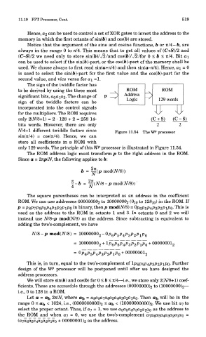
The sign of the twiddle factor has
to be derived by using the three most ROM ROM
significant bits, oooio 2. The change of 1 Address ~^ 129 words
Logic
sign of the twiddle factors can be '
incorporated into the control signals
for the multipliers. The ROM requires
only 2C/V/8+1) = 2 • 128 + 2 = 258 14- (C + S) (C-S)
bits words. However, there are only 2 2
M4+1 different twiddle factors since Figure 11.54 The W processor
sin(7t/4) = cos(rc/4). Hence, we can
store all coefficients in a ROM with
only 129 words. The principle of this WP processor is illustrated in Figure 11.54.
The ROM address logic must transform p to the right address in the ROM.
Since a = 2np/N, the following applies to 6:
b = 2*(p mod(A/78))
-pmod(JW8))'
The square parentheses can be interpreted as an address in the coefficient
ROM. We can use addresses 00000000 2 to 10000000 2 (Oi 0 to 128i 0 ) in the ROM. If
in
P =P8P7P6P5P4P3P2PlPO binary, thenp mod(M8) = Op 6p5P4P3P2PlPO- Tnis is
used as the address to the ROM in octants 1 and 3. In octants 0 and 2 we will
instead use N/8-p mod(M8) as the address. Since subtracting is equivalent to
adding the two's-complement, we have
N/8-p mod(A/78) = 10000000 2-0p 6p 5p 4p 3jp 2p 1p 0
= 10000000 00000001
This is, in turn, equal to the two's-complement of lpeP5P4.P3P2.PlPO- Further
design of the WP processor will be postponed until after we have designed the
address processors.
We will store sin(6) and cos(6) for 0 < 6 < Tt/4 — i.e., we store only 2(M8+1) coef-
ficients. These are accessible through the addresses (00000000) 2 to (10000000) 2—
i.e., 0 to 128 in a ROM.
a a a a a a a
Let a = at 2n/N, where a\y = a9fl8«7 6 5 4 3 2 l o- Then a^ will be in the
range 0 < o b < 1024, i.e., (0000000000) 2 < a\> < (10000000000) 2. We use bit 07 to
select the proper octant. Thus, if 07 = 1, we use 0605040302^100 as the address to
the ROM and when 07 = 0, we use the two's-complement 0705050403020100 =
(0705050403020100 + 00000001) 2 as the address.