
Page 537 - DSP Integrated Circuits
P. 537
522 Chapter 11 Processing Elements
11.19.5 RAM Address PEs
The address processors must compute the RAM addresses from the base index by
conditional setting of the extended bits. This can be accomplished by the unit
shown in Figure 11.57.
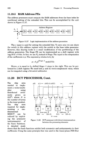
taddress Register
*1 1
^ D D D D ~* D -> D -> D -* D ~* D
- -
Figure 11.57 Logic implementation of the address generation
The e input is used for setting the extended bits. To save area we can share
the switch in this address register with the switch in the base index generator.
However, this sharing leads to a small modification of the partitioning of the
address generation. The Stage PE can be implemented as a shift register with
log2(M2) = 9 bits. In fact, we use N s instead of Stage. The input to the computation
of the coefficients is p. The exponent p relates to k\ by
Hence, p is equal to k\ shifted Stage-I steps to the right. This can be per-
formed in a shift register. We need both p and its two's-complement value, which
can be computed using a bit-serial subtractor.
11.20 DCT PROCESSOR, Cont.
The chip area x(N/2-\) x(N/2)
needed to imple-
ment a vector-multi-
plier using
distributed arith-
metic grows as
O(2^) where N is
the number of terms
in the inner product. T
The chip area I,,-,,
required for imple- •<*'•••,
menting a one- PE PE
dimensional T Even rows T Odd rows
MSDCT can be X(0) ... X(N-2)
reduced by exploit- N = even
ing the symmetry
Figure 11.58 DCT processor with direct interconnection
(antisymmetry) of between the processing elements
the basis functions.
A detailed study
shows that the basis functions exhibit both symmetry and antisymmetry in their
coefficients. Using the same principle that was used in the linear-phase FIR filter